This thread has been locked.

If you have a related question, please click the "Ask a related question" button in the top right corner. The newly created question will be automatically linked to this question.

BQ25622E: Buck Inductor choice - equations give much bigger value than typical circuit/EVM, which do I use?

Part Number: BQ25622E
Other Parts Discussed in Thread: BQ25622

Tool/software:

I am using the BQ25622E for an application with 12V input (nominal), single Li-ion output so 3.5V-4.2V output, and 1A charge current approx.

I have come to choose the buck circuit inductor using Equation 4 in the datasheet:
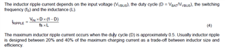
Nominal

Re-arrange Eq4 for L, assume 30% ripple of 1A output, and nominal input/output voltages;

D = V_BAT / V_BUS = 4V / 12V = 0.3333

L = VIN * D * (1 - D) / (fs * I_RIPPLE) = 12 * 0.3333 * 0.6666 / (1.5MHz * 0.3A) = 5.92uH

Worst Case

Re-arrange Eq4 for L, assume 20% ripple of 1A output, and worst case input/output voltages;

D = V_BAT / V_BUS = 4.2 / 18V = 0.2333

L = VIN * D * (1 - D) / (fs * I_RIPPLE) = 18 * 0.2333 * 0.7666 / (1.5MHz * 0.2A) = 10.73uH


Both of these are huge compared to the typical application circuit given in the datasheet, and the EVM circuit design which both use 1uH.

However both of those sources say they support the ranges I use (listed as up to 18V for input) so on one hand I should be able to just copy the same circuit and use the 1uH inductor size but viewing from another direction this should be 10x larger!

So a couple things;

  • Even accounting for this calculation being 1A charge current instead of the full 3A charge current, this still gives 2uH, so a 2.2uH part would be chosen. This is still a way away from the 1uH in the EVM and datasheet calculations - this is still only at 12V, before accounting for these circuits saying they are for use up to 18V at the input. Is there a mistake in the typical/EVM circuit (e.g. actually designed for 5V input only would make sense), or is there no mistake but just that it is OK for it to be stretched away from the ideal at other input/charge conditions?
  • Do I follow the calculation, or go with the typical circuit? The typical circuit should also cover my usage conditions but yet gives a hugely different inductor size to the calculation.


Thanks for any help

Kevin

  • Hi Kevin,

    We will check and get back to you soon.

    Thanks,

    Ning.

  • Thank you!

    Kevin

  • Also, the input capacitor is shown as 1uF typical, but in Section 9.2.2.2 Input Capacitor;

    "10-μF ceramic capacitor is suggested for typical of 3.5A charging current."

    The BQ25622E is only 3A max not 3.5A, is this note leftover from the BQ25622 (different part, without 'E' which has 3.5A)? What is the guidance for this part?

  • Hello Kevin

    Due to the U.S. holiday our responses may be delayed. We will respond by the end of the work week.

    Sincerely,

    Wyatt Keller

  • Hi Kevin,

    The charger device has internal loop compensation. The output inductance should be between 1uH to 2.2uH.

    Thanks,

    Ning.

  • Hi Ning,

    All buck devices have internal loop compensation, that doesn't mean anything.

    Please could you provide a reasoned answer in response to the questions asked and the calculations.

    If I should use 1uH, why? Are the datasheet equations wrong?

    Also there was the question of the input capacitor too which is given a conflicted value in the datasheet.

    Thanks

    Kevin

  • Hi Kevin,

    A buck converter power stage is open-loop. It needs feedback compensation network to be a closed-loop stable system. The feedback compensation network can be external for some DC/DC converters or controllers. Please visit Designing Stable Control Loops https://www.ti.com/seclit/ml/slup173/slup173.pdf for more details.

    From the system stability standpoint, it is recommended to use output inductance between 1uH to 2.2uH. The equations are correct. Customer may use their preferred output inductance as long as the charger performance meets their specific application requirements.

    Thanks,

    Ning.

  • Hi Ning,

    Yes, sorry, I was being too hyperbolic and dismissive as I don't see how that is answering the question asked. Yes, some compensation is external.

    You say "the equations are correct". Using the equations I get figures 10x higher than the 1uH suggested. There is an issue somewhere, either in my calculations, the datasheet, or my understanding of the reasoning.

    I would be remiss if I didn't understand this properly before completing the design. Hopefully you can help fill in this gap.

    Also again there was the question of the input capacitor too which is given a conflicted value in the datasheet.

    Kevin

  • Hi Kevin,

    1. There are several considerations for the output inductance. Trade-offs are needed. For this particular part, system stability should have higher priority than the output inductor ripple. So it is recommended to use output inductance between 1uH to 2.2uH. Again, customer may use their preferred output inductance as long as the charger performance meets their specific application requirements.

    2. For  the input capacitor, PMID is the actual charger input, so 10-uF is suggested. 1-uF cap is for VBUS.

    Thanks,

    Ning.

  • Thank you for your help Ning. All understood now cheers.

    Kevin