Tool/software:
Hello,
I'm designing a 3.6V 2A boost. I Have few question about the layout.
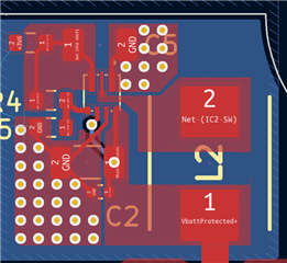
1) Is it the layout correct ? GND are connected via the GND area under the regulator (Layer 2 and Layer 4) :

2) I have doubts when I create a GND pour copper zone on Layer 1.
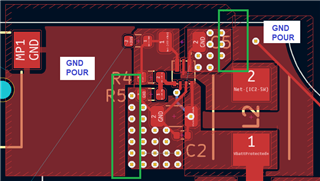
Do I have to keep the "GND areas near to the device" separated to the GND pour area (connected only via Layer 2 and Layer 4 that are not shown on this picture):

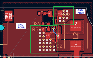
Or is it OK if the pour copper is connected to the "GND areas" near to the device (and also via Layer 2 and Layer 4 that are not shown on this picture):

Best regards,
Riccardo


