This thread has been locked.

If you have a related question, please click the "Ask a related question" button in the top right corner. The newly created question will be automatically linked to this question.

BQ40Z80: BQ76942: DSG FET turn off problem

Part Number: BQ40Z80

Tool/software:

Hello everyone,

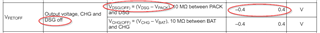
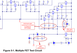
I'm using the bq40z80 chip in my project and I've encountered an issue. When I send the command to turn off the DSG pin, its voltage drops from 27 volts to around 13-14 volts instead of going to zero. As a result, there is always voltage present on the load. What am I doing wrong?

  • Hello,

    Today's a national holiday. We will get back to you tomorrow.

    Regards,

    TI Apps Team

  • Hello,

    The driver charge pump is about ~11V. It looks like your voltage drop is close to that. Where are you probing to check the turn-off voltage. You should be probing at DSG pin and at PACK+ (+Load)


    Also, it looks like the connection of the 10 Meg Ohm resistor is before the gate resistor. It should be after. I would check and compare your CHG and DSG FET connections with our EVM schematic. 


  • Hello,

    I connected the resistors R1 according to the above schematic and desoldered VT3 for testing. However, the voltage on pin 26 remains around 11 volts relative to GND, whereas according to the datasheet, it should be 0 volts when turned off. My battery is 16 volts, and when the turn-on command is given, the output on DSG is 27 volts relative to ground or 11 volts relative to the source, which is expected. However, when the turn-off command is given, the DSG pin remains at 13 volts relative to ground or about 2.5 volts relative to the source, causing the transistor to enter the linear mode and not fully turn off. I expect it to be 0 volts relative to ground.

    Thank you.

  • Hello,

    To determine if DSG FET is off, you should be probing between DSG pin and the connection of your load (Load+). This voltage should be around 0V for fully FET off. When ON, this voltage should be around 11V (charge pump voltage). Please see below. 

    You should not be probing with respect to GND.


    It looks like somehow in your circuit something is causing an extra 2V between the gate of DSG pin and the Load+ (Vgs). 
    I would assume it is due to the 10 Meg Ohm (R1) resistor being before and not after R2.

    Looks like you have parallel FET connection. Please see below for reference on parallels FETs. 
    REFERENCE:
    https://www.ti.com/lit/an/sluaa09a/sluaa09a.pdf

    https://www.ti.com/lit/ab/slpa020/slpa020.pdf