LP87564-Q1: LP87564-Q1 PGOOD signal.

Part Number: LP87564-Q1
Other Parts Discussed in Thread: LP87564Q1EVM

Tool/software:

Hello All

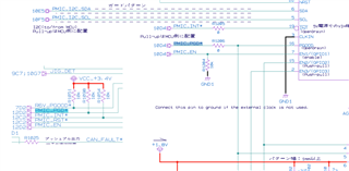
We used the LP87564-Q1 for the FPGA power supply and prototyped an OTP product.
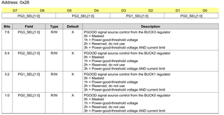
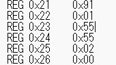
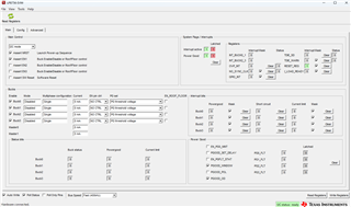
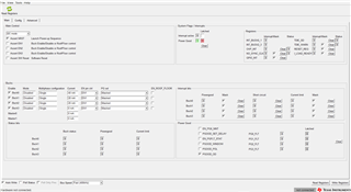
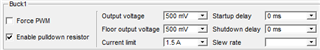
The PGOOD register is set to mask.

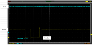
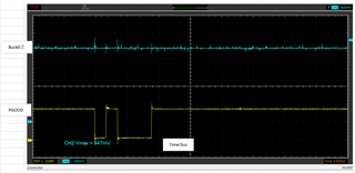
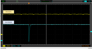
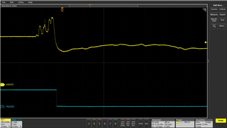
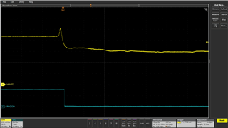
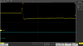
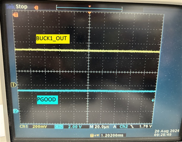
Nevertheless, the PGOOD signal is output.
The output waveform is 10us, which is much shorter than a normal PGOOD signal.

I guessed that this signal was a glitch in the IC's internal gate circuit.

Please let us know what you think.

Thanks in advance

Hiroyuki

  • Hi Hiroyuki,

    Are you working with an FAE over this issue? Your buck 2 waveform is seeing 947mV max in the capture correct?

    Thanks,
    Field

  • Hi Fleld,

    Thank you for reply.

    Indeed, I am communicating with the FAE at TI Japan about this issue.
    I am attaching the Buck2 waveform, and I was also concerned about the high noise level.

    However, what I want to know is why the PGOOD register is masked but a 10us signal is output.

    Thanks,

    Hiroyuki

  • Hi Hiroyuki,

    Okay I just wanted to make sure that this was the same issue Slight smile

    Can you tell me the full orderable part number that you are using? Are you sending any reads/writes to the registers? What is the process that you are doing to get to this point, and what state is the device in? Before this (or enabling the device) it may be helpful if you can read each of the registers and provide this to me.

    Thanks,
    Field

  • Hi Fleld,

    I have attached two files.
    "LP8756B2_0x111.txt "is the instructions for ordering the OTP.
    It contains the detailed part number.
    "Actual register.txt" is the register file read from the PMIC of the board we are considering.

    We appreciate your cooperation.

    Thanks,

    Hiroyuki

    Actual register.txt
    REG 0x00	0x92
    REG 0x01	0x11
    REG 0x02	0xC6
    REG 0x03	0x0E
    REG 0x04	0xC6
    REG 0x05	0x3E
    REG 0x06	0xC6
    REG 0x07	0x2E
    REG 0x08	0xC6
    REG 0x09	0x0D
    REG 0x0A	0x61
    REG 0x0B	0x00
    REG 0x0C	0x2F
    REG 0x0D	0x00
    REG 0x0E	0x2F
    REG 0x0F	0x00
    REG 0x10	0xB1
    REG 0x11	0x00
    REG 0x12	0x23
    REG 0x13	0x50
    REG 0x14	0x41
    REG 0x15	0x32
    REG 0x16	0x14
    REG 0x17	0x05
    REG 0x18	0x00
    REG 0x19	0x5E
    REG 0x1A	0x00
    REG 0x1B	0x00
    REG 0x1C	0x00
    REG 0x1D	0x00
    REG 0x1E	0x00
    REG 0x1F	0xCC
    REG 0x20	0xCC
    REG 0x21	0x91
    REG 0x22	0x01
    REG 0x23	0x55
    REG 0x24	0x55
    REG 0x25	0x02
    REG 0x26	0x00
    REG 0x27	0x1A
    REG 0x28	0xC0
    REG 0x29	0x12
    REG 0x2A	0x00
    REG 0x2B	0x01
    REG 0x2C	0xD6
    REG 0x2D	0x06
    REG 0x2E	0x06
    REG 0x2F	0x06
    
    LP8756B2_0x111.txt
    device: LP8756B2.dev
    name: LP87564WRNFRQ1
    description:
     // LP8756/52/57 OTP Configuration File
    // Silicon version: B2
    // Configuration: 1+1+1+1
    // OTP ID: 0x111
    // Customer: Melco
    // Generated: 12/09/2022 08:41:48
    // 
    // Beginning of Selectable OTP Configuration Bits
    // 
    <LREGS>
    DEVICE_ID: 2
    OTP_ID: 17
    EN_BUCK0: 1
    EN_PIN_CTRL0: 1
    BUCK0_EN_PIN_SELECT: 0
    BUCK0_FPWM: 1
    BUCK0_FPWM_MP: 0
    ILIM0: 1
    SLEW_RATE0: 6
    EN_BUCK1: 1
    EN_PIN_CTRL1: 1
    BUCK1_EN_PIN_SELECT: 0
    BUCK1_FPWM: 1
    ILIM1: 7
    SLEW_RATE1: 6
    EN_BUCK2: 1
    EN_PIN_CTRL2: 1
    BUCK2_EN_PIN_SELECT: 0
    BUCK2_FPWM: 1
    BUCK2_FPWM_MP: 0
    ILIM2: 5
    SLEW_RATE2: 6
    EN_BUCK3: 1
    EN_PIN_CTRL3: 1
    BUCK3_EN_PIN_SELECT: 0
    BUCK3_FPWM: 1
    ILIM3: 1
    SLEW_RATE3: 5
    BUCK0_VSET: 97
    BUCK1_VSET: 47
    BUCK2_VSET: 47
    BUCK3_VSET: 177
    BUCK0_SHUTDOWN_DELAY: 2
    BUCK0_STARTUP_DELAY: 3
    BUCK1_SHUTDOWN_DELAY: 5
    BUCK1_STARTUP_DELAY: 0
    BUCK2_SHUTDOWN_DELAY: 4
    BUCK2_STARTUP_DELAY: 1
    BUCK3_SHUTDOWN_DELAY: 3
    BUCK3_STARTUP_DELAY: 2
    GPIO2_SHUTDOWN_DELAY: 1
    GPIO2_STARTUP_DELAY: 4
    GPIO3_SHUTDOWN_DELAY: 0
    GPIO3_STARTUP_DELAY: 5
    DOUBLE_DELAY: 0
    CLKIN_PD: 1
    EN4_PD: 0
    EN3_PD: 1
    TDIE_WARN_LEVEL: 1
    EN2_PD: 1
    EN1_PD: 1
    GPIO_MASK: 1
    SYNC_CLK_MASK: 1
    TDIE_WARN_MASK: 0
    I_LOAD_READY_MASK: 1
    RESET_REG_MASK: 1
    BUCK1_PG_MASK: 1
    BUCK1_ILIM_MASK: 1
    BUCK0_PG_MASK: 1
    BUCK0_ILIM_MASK: 1
    BUCK3_PG_MASK: 1
    BUCK3_ILIM_MASK: 1
    BUCK2_PG_MASK: 1
    BUCK2_ILIM_MASK: 1
    PG3_SEL: 3
    PG2_SEL: 3
    PG1_SEL: 3
    PG0_SEL: 3
    HALF_DELAY: 0
    EN_PG0_NINT: 0
    PGOOD_SET_DELAY: 0
    EN_PGFLT_STAT: 0
    PGOOD_WINDOW: 0
    PGOOD_OD: 1
    PGOOD_POL: 0
    PLL_MODE: 0
    EXT_CLK_FREQ: 1
    EN_SPREAD_SPEC: 1
    EN_PIN_CTRL_GPIO3: 1
    EN_PIN_SELECT_GPIO3: 0
    EN_PIN_CTRL_GPIO2: 1
    EN_PIN_SELECT_GPIO2: 0
    GPIO3_SEL: 1
    GPIO2_SEL: 1
    GPIO1_SEL: 0
    GPIO3_OD: 0
    GPIO2_OD: 0
    GPIO1_OD: 0
    GPIO3_DIR: 1
    GPIO2_DIR: 1
    GPIO1_DIR: 0
    GPIO3_OUT: 1
    GPIO2_OUT: 1
    FOUR_ENABLE_MODE: 0
    I2C_HS: 0
    DIS_EN2_OTP_READ: 1
    BUCK_FREQ_SEL: 0
    I2C_ID_SEL: 0
    EN_OVP: 1
    MULTIPHASE_CONFIGURATION: 1
    I2C_ID: 97
    BUCK1_SC_MASK: 0
    BUCK0_SC_MASK: 0
    BUCK3_SC_MASK: 0
    BUCK2_SC_MASK: 0
    EN_FRAC_DIV: 0
    EN_P_10M_BODY_DIODE: 1
    EN_PROPORTIONAL_CHOKE_CONTROL: 1
    EN_HIGH_FREQ_NEG_OCP: 0
    EN_WAIT_CURRENTS_BALANCED: 1
    EN_PREVENT_PHASE_ADD: 1
    PROPORTIONAL_COEFF_BUCK: 4
    COMPENSATING_RAMP_SLOPE: 5
    ENABLE_CURRENT_BALANCING: 1
    LONG_SINGLE_SHOT: 0
    DIS_VREF_DAC_WAIT_P10M: 0
    EN_INT_CHOKE_CTRL: 1
    SET_NEG_I_COMP_OFFSET: 0
    PFM_IPEAK: 19
    PHASE_SHED_NEG_LIMIT: 0
    IND_NEG_LIMIT: 1
    EN_POS_NEG_OCP: 1
    EN_SHED_PHASE_INT_CONTROL: 0
    PFM_ENTRY_BUCK: 1
    ADD_PHASES: 2
    SHED_PHASES: 2
    ADC_10M_WORD: 1
    ADC_M0M_WORD: 2
    ADC_P0M_WORD: 3
    PLL_ICP_SEL: 1
    EN_TWARN_DISABLES_BUCKS: 0
    FORCE_SINK_BUCK3: 0
    FORCE_SINK_BUCK2: 0
    FORCE_SINK_BUCK1: 0
    FORCE_SINK_BUCK0: 0
    DIS_UVLO: 0
    RESET_PREVENTS_STARTUP: 0
    DIS_TSDH: 0
    EN_BUCK_ENABLE_SHIFTER: 1
    IDAC_LSB: 0
    SLAVE_INTEGRATOR_STEP_DELAY: 1
    POS_OCP_LEVEL_MSB: 0
    PFM_IPEAK_RETENTION: 2
    EN_RETENTION_MODE: 0
    EN_10M_PROP_CONTROL: 0
    EN_PG_COMPARATORS: 1
    

  • Hi Hiroyuki,

    And can you tell me how you are arriving to this point? Is this on start up, shutdown, enabling the device, etc? Does it happen once, or every time during this aforementioned portion/process? Are you changing any of the registers, and if so at what point and what is the occurrence?

    One thing that may stand out is register 0x29:

    This would imply that the following bit below would be a 1 value for your board but in the OTP for this device, this bit looks like it is set to a 0, so I am a little confused on the above questions regarding the process or attempts that have been made so far. Register below:

    Could you try again (with setting the masks accordingly), but set this bit to a value of 0 instead and inform me of the results? And let me know what you may have tested or changed previously in working with this?

    Thanks,
    Field

  • Hi Fleld-san,

    The problem probably became more noticeable after updating the SoC firmware.
    Since updated the firmware, the transient current consumption seems to have increased.
    The SoC kernel starts and PGOOD periodically asserts low.
    We will be testing register 0x29 soon, please wait a day or two.
    Change the register value from 0x12 to 0x00?

    Thanks,

    Hiroyuki

  • Hi Hiroyuki,

    So this is seen just during normal operation when a load is present? 

    Are you changing any of the registers, and if so at what point and what is the occurrence?

    Assuming the register dump you provided is after (and if) you have written to the registers and the corresponding masks are present. Could you try a value of 0x02 to this register 0x29? 

    Thanks,
    Field

  • Hi Fleld-san,

    Yes, this occurs during normal operation under load.

    Thanks,

    Hiroyuki

  • Hi Fleld-san,

    I have tested 0x29=0x02 and 0x28=0x00 and the PGOOD signal still asserts.

    If there are any other registers to test, please advise.

    Thanks,

    Hiroyuki

  • Hi Hiroyuki-san,

    Field moved to a new position in TI. Let me look into this for you and I will reply by tomorrow (7/16).

    Sorry for the delay,

    Matt

  • Hi Hiroyuki-san,

    Can you please capture the output rails along with the PGOOD signal in the oscilloscope capture? It would be good to see if there is any noise that might be causing PGOOD to trigger.

    Best regards,

    Matt

  • Hi Matt-san,

    Please refer to the previous post.
    I am capturing Buck2 and PGOOD signals,
    This waveform looks noisy.

    I think PGOOD is asserted because the overvoltage threshold has been exceeded.

    However, even if I mask PG_SEL with 0h, this signal still appears,
    so this doesn't make sense to me.

    If you could explain the mechanism by which the signal appears even when PG_SEL is masked.

    Best regards,

    Hiroyuki

  • Hi Hiroyuki-san,

    Can you let me know which register is being selected with this mask bit? I will dig into this more tomorrow - I think the mask bit might affect the INT pin, but I need to study this more to make sure.

    Thanks,

    Matt

  • Hi Mattsan,

    I asked a TI Japan FAE about the register mask settings and did it carefully.

    0x28=0x00   

    FAE said that with this setting, PDOOD is masked and no signal is output.

    Best regards,

    Hiroyuki

  • Hi Hiroyuki,

    Has the PGOOD_FLT register been cleared also after writing to the register mask settings?

    Regards,

    Matt

  • Hi Matt-san,

    The current OTP is 0x23=0x55, 0x24=0x55. This register setting does not latch the interrupt.
    Therefore, there is no need to clear the GOOD_FLT register.

    Best regards,

    Hiroyuki

  • Hi Hiroyuki,

    Let me ask some other engineers from the team to see if they can help understand what you are describing. I apologize for the delay and hope to reply on Monday with suggested next steps.

    Best regards,

    Matt

  • Hi HIroyuki-san,

    I was looking at the value of the 0x16 register - I think I may suggest some changes to this register to see if it affects the behavior.

  • Hi Matt-san,

    Are there any specific instructions for Register 0x16h?

    The current OTP Register setting is 0x16=0x14.

    In my opinion, 0x16 is a register for setting the GPIO delay step and has nothing to do with PGOOD.

    Best regards,

    Hiroyuki

  • Hello Hiroyuki-san, 

    Sorry, Matt is currently out of office until Monday 7/29.
    He or I will try to get back to you by then. 
    Thank you for your patience.

    Best Regards,
    Sarah

  • Hi Sarah-san and Matt-san,

    I hope the results of my analysis today will provide some clues.

    I loaded our product's OTP into the LP87564Q1EVM, and the PGOOD status latched.
    It seems that PGOOD is always asserted, as it latches immediately even after clearing it.
    The load on the EVM is zero.

    I would like you to carefully re-examine the OTO "Actual register.txt" that I sent to Fleld previously.

    Best regards,

    Hiroyuki

  • Hi Sarah-san and Matt-san,

    Further experimental results:
    Using the LP87564Q1EVM GUI, I changed the output voltage of OUT1 from 850mV to 855mV,
    and the PGOOD was asserted.
    Is this device really that sensitive?

     waveform:
    A change of 5mV cannot be measured at 200mV/div.

    Best regards,

    Hiroyuki

  • Hi Hiroyuki-san,

    Thank you for providing your own experimentation results, this is certainly unexpected behavior. 

    I do not immediately see any issues with the register settings other than what has already been mentioned by Field and the FAE,
    but let me see if I can replicate this setup on my end to further test and troubleshoot the issues. 
    I will get back to you with my findings. 

    Best regards,
    Sarah

  • Hi Sarah-san and Matt-san,

    Is the testing progressing?
    Please let us know the status.

    Best regards,

    Hiroyuki

  • Hi Hiroyuki-san, 

    Apologies for the delay, it took longer than expected to receive the samples on hand. Testing will begin immediately and I will let you know what I find. 
    So sorry for the long wait.

    Best regards, 
    Sarah

  • Hello Hiroyuki-san, 

    Apologies, we are still conducting testing on our end and are awaiting a soldering job, I will try to get back to you by tomorrow.

    Again, I am sorry for the long delay.

    Best, 
    Sarah

  • Hi Sarah-san,

    Our company will be on summer vacation from Aug.9 to Aug.18.
    We apologize for not being able to contact you during this period.

    Best regards,

    Hiroyuki

  • Hi Hiroyuki-san,

    So far we did a simple check to see if the PG_SEL masking options were working with the EVM and we found that when BUCK2 PG2_SEL = 0, the PGOOD pin was not being pulled LOW by a BUCK2 PGOOD fault. This indicates that the mask setting is working.

    This is what our GUI looks like before we run the test. We have PGOOD masked for all BUCKs: 

    One thing I would like point out is that the "Power Good" system flag at the top will show 1'b for both the flag and the latched bit whenever one of the BUCKs is reporting PGOOD. This is normal and does not indicate a PGOOD issue. This flag bit is set to indicate that the output power of the PMIC is currently within regulation. The interrupt bit will show when a problem has occurred on a BUCK.

    Even when PGOOD is masked, you will see 1'b for "Power Good" at the top of the GUI.

    I still want to try and confirm that overvoltage specifically should not trigger PGOOD to go LOW when PGOOD is masked for BUCK2 but so far our testing shows that the mask bit should prevent PGOOD from going LOW.

    Regards,

    James

  • Hi Hiroyuki-san,

    Can you share your schematic here as well?

    What is the pull-up source for PGOOD?

    Regards,

    James

  • Hi James-san,

    Thank you for testing so quickly.
    Is there a waveform where PGOOD is not pulled low?
    It is a short pulse of about 10us.
    Please observe with the trigger set to normal or single.

    This is an excerpt of the PGOOD pull-up circuit.
    This is confidential information so I can't show you the whole thing.
    PGOOD is pulled up to the CPU's VDD (+3.4V).

    Best regards,

    Hiroyuki

  • Hi James-san,

    Let me confirm one more thing.
    Please also observe the PGOOD signal when the GUI PG sel setting is "3h = Power-good-threshold voltage AND current limit".

    Best regards,

    Hiroyuki

  • Hi Hiroyuki-san,

    Currently working on that scope capture.

    Field mentioned register 0x29 earlier in this thread. Did you already test setting register 0x29 bit 5 = 1'b? This will set the PGOOD debounce delay to 1-11ms instead of 4-8us.

    If your PGOOD is being pulled low due to periodic noise on BUCK2, the longer de-bounce time might be enough to ignore the noise spikes, so try changing that bit if you haven't already and let me know if that makes any difference.

    If I can get a good image of PGOOD testing with and without masking bits I'll post it in a follow up reply.

    Regards,

    James

  • Hi Hiroyuki-san,

    Here are some scope captures of the PGOOD behavior I'm seeing. It's difficult to induce the exact same noise behavior you experienced on your end so I had to settle with shorting the FB pathway to create an erratic BUCK2 output.

    1) PGOOD is NOT masked, monitoring PG threshold only (overvoltage AND undervoltage)

    2) PGOOD is NOT masked, monitoring PG threshold AND current limit (overvoltage and undervoltage)

    3) PGOOD is MASKED in all PG_SEL registers, PG is still set for overvoltage and undervoltage but expectation is that PGOOD will remain HIGH even during short event.

    Regards,

    James