This thread has been locked.

If you have a related question, please click the "Ask a related question" button in the top right corner. The newly created question will be automatically linked to this question.

UCC28070: The input AC waveform is distorted when loading

Part Number: UCC28070
Other Parts Discussed in Thread: UCC27624

Tool/software:

HI 

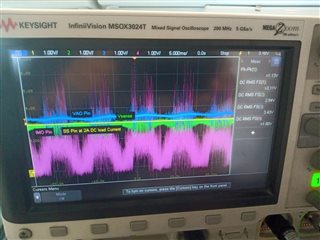
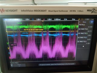
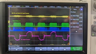
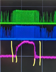
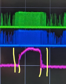
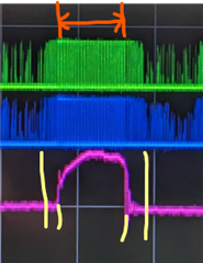
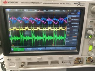
I am Testing a 3.3kw interleaved PFC using UCC28070

Input AC voltage: 230, 50HZ

the output voltage is 400V regulated by IC

But As I am loading the PFC to the current waveform is becoming more of a square type and PF is becoming less. What could be the problem 

I can share the schematics in mail ID 

  • Hello Hema, 

    The waveform shown with long "deadtime" around the zero-crossing suggests to me that your DMAX resistor value is too low, causing a low maximum allowable duty cycle. 

    The dead time may always be there, but at light loads, the line current peak is lower so it may not appear to be very square.  But at higher loads, the center peak has to rise and the overall input current looks more "square" as the load increases.   

    If that is not the case, another possibility is that you have too much offset voltage on the CSA and CSB signals.
    Please check to see if there is more than about 100~120mV DC offset voltage on these signals.  If so, please reduce it.  Sometimes no offset at all is necessary. 

    Regards,
    Ulrich 

  • HI Ulrich

    The Dmax resistor value was high enough for the Duty cycle of 94 percent 

    I have decreased the offset voltage from 200mV to 100mV for the current sense but still, the waveform is not improved 

  • Hello Hema, 

    Thank you for the schematic file. It is helpful. 
    Several of the components around the PFC controller have two values listed: one in black text, one in red text in parentheses.  Which of the values should be applied to your design? 

    Reviewing your waveforms again, I see that the "O/P current" (CH4) has humps that correspond to the humps in the AC input current, and it has flat spots that correspond to the zero parts of the AC input current.  But the DC O/P flat sections are not zero current, so the PFC power stage appears to be getting input power from a DC source of some voltage between 0V and the AC line peak.  Can you please check for this? 

    Also, where is the O/P current probe located? 

    Regards,
    Ulrich

  • The text with black ones is mounted on the board. 

  • The output is connected to an electronic load with a  CC current of 2.5A  and the current probe is connected around  a DC positive wire which is  connected between pfc output and electronic load

  • Hello Hema, 

    Thanks for your replies.  
    I am trying to make sense out of the O/P current waveform based on your load description. 
    A CC load should show as steady-state DC current, with little or no AC ripple.  Your waveform has a lot of AC ripple.

    The only way I can make sense of this is to envision that you have substantial output capacitance at the e-load end of the positive wire, and the current probe is measuring the ripple current into that capacitance.  The e-load current itself may be strictly-flat DC, but the probe is not measuring that. 
    Can you check for that situation, please?

    Aside from that, can you also capture SS-pin, VSENSE-pin, VAO-pin, and IMO-pin voltages all at 1V/div with zero-references all on the same horizontal line, please?  Set time sweep to 5ms/div.  Use the same input and output test conditions as in your screen-capture, above. 

    'Scope bandwidth limit can be 20MHz (or lower) to reduce noise, and use tip & barrel probing if BW limit does not clean up the signals enough. 

    Regards,
    Ulrich

  • Hi Ulrich,

    As per your suggestion, we captured the SS-pin, VSENSE-pin, VAO-pin, and IMO-pin voltages at 1V/div at 5ms/div. The E_load is loaded at 2A DC.

    The IMO pin has more voltage spikes, corresponding wave (IMage2_ zero reference with all on the same horizontal plane, IMag1_at different plane) form is attached for your reference. 

    Regards,

    Harinaik Sugali.

  • Hello Harinaik, 

    Thank you for the waveforms.  They are very noisy, but I do see an issue. 
    The SS voltage should not be stuck at 3V, but it should be up close to 6V.  Please check to see what is preventing SS from rising and remove the problem. 

    Regards,
    Ulrich

  • Hi Ulrich,

    Thank you for the valuable information.

  • Hi Ulrich,

    The SS-pin voltage is more than 5V, but the issue is not yet resoled. The AC input current wave form is distorted (non sinusoidal). For your kind reference, the experimental result at light load is attached. What could be the issue?

  • Hello Sugali, 

    I wish the cause was the SS pin voltage stuck at 3V, but since it isn't we'll have to look further. 

    This is a strange situation that I don't understand. In the picture below, we can see gate drive pulses before and after the edges of the input current waveform.

    Where there are gate drive pulses, I expect to see MOSFET switching.  Where the MOSFETs are switching I expect to see inductor current.  When there is inductor current, I expect to see the average of that current at the AC input.  Above, we are seeing gate-drive with no current. 
    Please investigate this chain of events to verify if the inductors are conducting current or not in the intervals between the yellow lines. 

    I have a number of additional questions:
    1.  Two days ago, I asked Hema if there was a lot of capacitance at the E-load end of the DC output cable.  Please answer that question so that I can account for the shape of the O/P current waveform in his original post.  
    2.  What kind of current probe are you using for these measurements?  
    3.  Does the average current in the boost inductors follow the same shape as the I/P current?  
    4.  Is the I/P voltage sinusoidal, or does it have the same shape as the I/P current? 
    5.  Please verify that bias power to the gate-driver IC (U200) is not being interrupted. 
    6.  Also please connect ENA and ENB signals on U200 to VDD (+15V_PS1) to ensure that noise cannot disable the output drivers.
    7.  By the way, the Mouser Electronics distributor indicates that this driver IC "2EDN8524R" is not recommended for new design. 

    Regards,
    Ulrich 

  • Hi Ulrich,

    Thank you for your valuable insights. Here I'm addressing your questions.

    1. The calculated output capacitor is 900uF, and selected value is 4*470uF=1880uF. Initially we have tested with 1880uF and changed to 3*470uF=1410uF.

    Even in both cases the AC input current is distorted.

    2. To measure the current, we are using the KEYSIGHT 1146B, 100kHz (@3dB), 0-70A RMS current probe.

    3. The boost inductor current wave form is more noise. Corresponding boost inductor current wave form and voltage across the CSA & CSB pin is given below image. The Phase _ A inductor current (Blue color) and Phase _ B inductor current (Pink color). The CSA pin voltage (Yellow color) and CSB pin voltage (green color). The voltage at CSB pin is more noise. 

    4. The input voltage is sinusoidal, but input AC current only distorted.

    5. Bias supply for gate driver IC (U200) is given from DC power supply (15V).

    6. We connected ENA and ENB signals on U200 to VDD (+15V_PS1) by shorting R235 & R236. Even though there is no improvement in the AC input current wave form. 

    7. We were used TI UCC27624 30V, 5A, Dual-Channel, Low-Side Gate Driver also. Even there is no improvement in the AC input current.

    Regards,

    Harinaik Sugali

  • Hi Harinaik,

    Thank you for your replies.  For each item: 

    1.  I was asking WHERE the capacitance is(was) located with respect to the current probe, although I do appreciate receiving the updated value information.
    My concern is whether most or all of the PFC output capacitance (Cout) was located after the current probe, because the output current waveform does not make sense to me if all of Cout is(was) before the probe.  
    2.  The KEYSIGHT 1146B probe is suitable for low frequency AC (<10kHz) and DC current measurements, but it is not suitable for switching frequency cycle-by-cycle measurements.  It will not show the correct ripple current in the inductors, nor the correct currents in the MOSFETs, etc.  You will need a probe with much higher bandwidth (>50MHz) for switching cycle measurements. 
    3.  I am unable to open the image file that you posted as a reply to my item 3.  Can you please repost the file, maybe as a .png file? 
    However, I don't want to see the CSx waveforms, I want to see the two inductor currents compared to the AC input current. 

    You can also capture the CSx signals in a different screen-shot. But if the CSx signals are very noisy, please use tip & barrel probing across the sense resistor(s) for cleaner signals.  See ref: https://www.analog.com/media/en/technical-documentation/application-notes/an-1144.pdf 
    4., 5.  Thank you.
    6., 7.  Thank you.  If the gate-drivers stay enabled and always deliver a gate pulse without reduced width when they receive an input pulse, then the drivers are not responsible for introducing distortion into the AC current.    

    I am still looking for the reason that the AC current is zero even while there are gate-drive pulses in this snippet from 4 days ago.  

    I have to assume that when the AC input current is zero, then the inductor currents are also zero, and I'd like to see waveforms that confirm this.  
    Assuming that is the case, the question becomes Why does the inductor current go to zero when there still are gate pulses?

    Regards,
    Ulrich 

  • Hi Ulrich,

    Thank you for the insights. 

    1. The output current probe is connected after the PFC output capacitor (Cout).

    In the below image, when the gate pulses are regular, AC input current is present (The orange color region) and in yellow area, gate pulses are irregular. 

    3. As per your suggestion, here I'm attaching  AC input current wave form with both inductor currents. Please refer the below Image.

    The boost inductor current wave form has more ripple. Corresponding boost inductor current wave form and voltage across the CSA & CSB pin is given below image. The Phase _ A inductor current (Blue color) and Phase _ B inductor current (Pink color). The CSA pin voltage (Yellow color) and CSB pin voltage (green color). The voltage at CSB pin is more noise.

    And we also observed that, the time duration of zero AC input current is constant even if we increase the load current. For your understanding, here we attached two images with load current of 1.5A DC & 2A DC. In these two cases, for 5.4ms AC input current is zero. Even at very light load, the time duration is same. But, the quality of the waveform is improved as load current increases.


    What would be the problem for this distorted waveform. 

    Regards,

    Harinaik Sugali

  • Hello Harinaik,

    Thank you for the additional waveforms.   The middle one with the CSA and CSB waveforms concerns me.  Those signals don't look anything like the inductor currents.  Those have to be investigated and fixed so that the CAx voltage signals proportionately match the rising inductor currents. 
    The inductor currents look like about 3A average with ~1A ripple.  Each CSx signal voltage should = 3A / Nct * Rs.  If they are not, find out why and fix it. 
    In my previous reply, I posted a link to a file that described how to make tip&barrel measurements to avoid picking up all kinds of switching noise.  Please follow that recommendation.  

    The inductor currents themselves have a surprising amount of high frequency ringing superimposed on the switching ripple. Can you please verify if that ringing current is real or if it is due to noise pick-up by the probes or 'scope grounding or some problem like that?  There should not be that kind of ringing in the current. 

    I wanted to refer back to the schematic diagram that was posted by Hema Danda on or around July 9.  However that schematic file has been removed. 
    Can you please post it again?  It is important to be able to discuss specific components.    

    I had wanted to refer to the offset components attached to the CSx signals.  In my July 8th post, I suggested to reduce the offset voltage if it was higher than ~120mV.  I also mentioned that it may not need any offset at all.  Hema responded that it had been at 200mV, but he reduced it to 100mV and there was no significant change.  Apparently, 0mV offset was not tested.  
    I now suggest to eliminate all of the offset and PWM-ramp circuits that are attached to the CSA and CSB signals.  Zero offset and zero ramp.   
    Please see if that makes a difference in the input current shape. 

    Regards,
    Ulrich

  • Hi Uirich,

    Thank you for the valuable comments.

    As per your suggestion, I have removed all of the offset and PWM-ramp circuit. 

    Case-I

    At this time, sense resister value is 100 Ohm ( in schematic R201, R202), and corresponding waveforms is attached below. Here, AC input current is improved and more noise is coming, but output voltage is dropping as load current increases. At this instant, phase A pulses are discontinues, compared to phase B. What would be the reason for discontinuous gate pulse.   

    Case-II

    In this case, the sense resister value is changed to 21 Ohm ( in schematic R201, R202) as per calculation. Here, AC input current waveform is again distorted and the gate pulse at phase A is not coming. The corresponding waveform is shown in below figure.

    What would be the issue here?? Whether current sense circuit or any other issue?


  • Hello Harinaik, 

    These waveforms don't make any sense to me.  I have never seen behavior like this.  
    Something is definitely wrong on the prototype board, but I can't think of what the cause can be. 

    You refer to R201 and R202 in the schematic, but the schematic has been removed.
    Please post it again.  

    Regards,
    Ulrich

  • Hi Ulrich,

    I have shared the schematic to your mail. Kindly refer it.

  • Hello Sugali, 

    I have received the file.  I will review it tomorrow.

    Regards,
    Ulrich