Tool/software:
Hello,
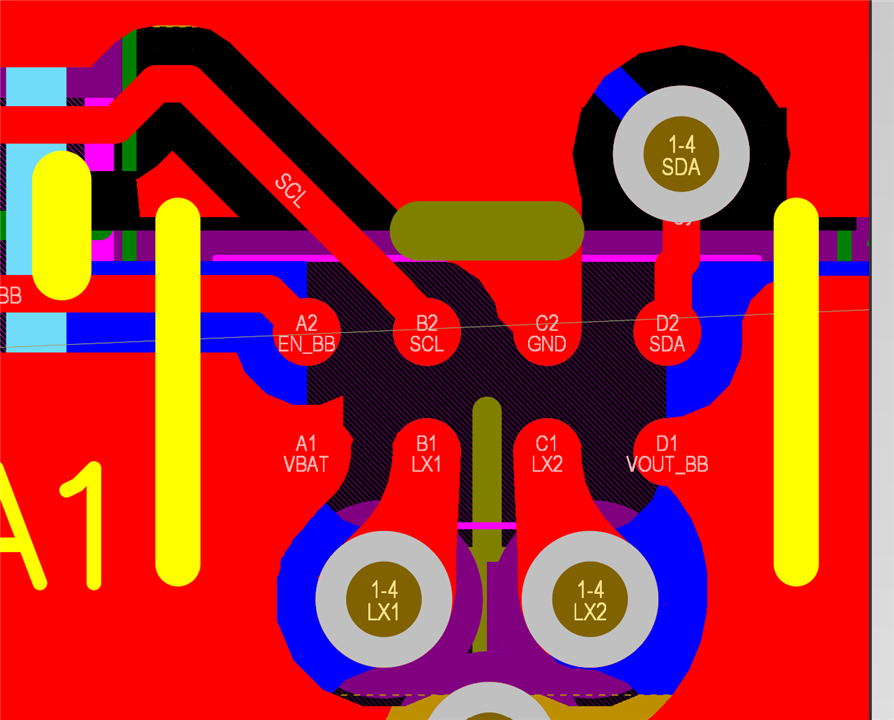
For a space-constrained design, due to routing, I intend to put a shielded 1uH inductor on the opposite side of the converter using several plated and conductive filled-vias.
At the moment, I am in prototyping and the fab only offers 10mil drill, so I am using 2 single 10mil drills to via.
My thought process is this would be OK since the topology of buck-boost, i am not affecting the loop area of the VOUT node, particularly with several vias which will reduce the series inductance condtributed by the vias.
I am curious on your thoughts on this approach and whether there are any other considerations i have missed.
Please see example layout below.