This thread has been locked.

If you have a related question, please click the "Ask a related question" button in the top right corner. The newly created question will be automatically linked to this question.

LMG3411R070: Power management forum

Part Number: LMG3411R070

Tool/software:

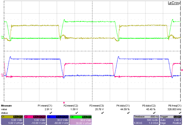
Hello, I'm Gunhee, and I'm developing a 1kw class LLC converter. I'm currently in charge of LLC converter on a 2nd stage PCB board with PFC and LLC. I see a phenomenon in which the high side input signal goes off for a month and then goes up to a positive voltage, and a strange waveform that goes down to a negative voltage before the input signal is turned on. When the input DC link voltage is increased, the positive and negative voltage magnitudes also increase, and the DC link voltage cannot be raised. That phenomenon is observed in all signals made based on SW nodes, such as LDO5V and VDD12V. Can you help me see which part is the problem? The low side input signal is good. I'm attaching a picture just in case it might be a PCB layout problem. I'm attaching a picture of the waveform as well.

CH1:High side input signal

CH2:Low side input signal

CH3:Low side Vds

CH4:High side Vds

231128_1kWCHG.PcbDoc

  • Hi, 

    How are the SW-referenced signals being measured? What types of probes are being used?

    The footprint in the PCB file is different than the LMG341xRxx footprint. Please make it match the footprint recommendation in the datasheet.

    The half-bridge layout does not follow the recommendations in Figure 19. The issues you are seeing could be related to 1. signal ground connection for the signal components 2. the wide loop of the ground return path or 3. the layout of the digital isolator IN signal. It is hard to tell where the IN signal is coming from. 

    Please revise the layout according to the recommendations outlined in the datasheet. 

     Thanks,

    John

  • Currently, I'm probing high side signals with a differential probe.

    I'm going to check the difference between LMG341X parts and half-bridge PCB layout guide and find out the cause by grinding the current PCB part. I'll ask you if I find additional problems. Thank you for your good response, Gomez.