This thread has been locked.

If you have a related question, please click the "Ask a related question" button in the top right corner. The newly created question will be automatically linked to this question.

TPS65400: SW2 output regulation error

Part Number: TPS65400

Tool/software:

Hello,

I am triyng to use TPS65400 for generating 4 indipendent voltages, each one with different regulation; in general Ioutmax = 0.3A and Vout = 7...9V. The control of the Ic is made with I2C protocol.

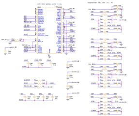
The schematic is attached as image. GND_POWER and AGND are connected in one point below the IC.

/resized-image/__size/320x240/__key/communityserver-discussions-components-files/196/5417.Immagine.png

Automatic start-up with external soft start and default sequencing order and timings. All switching frequencies set to defualt with divider 1.

All settings of the TPS are as default excect the one i will mention later.

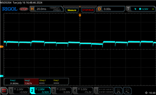
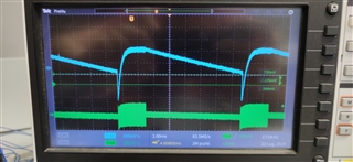
The problem I am facing is the following: after startup all 4 output voltages are correct with defualt vref (5.6V); when i change the vref value (to 48 decimal) buck 1 and 2 start behaving badly, while buck  3 and work correctly.

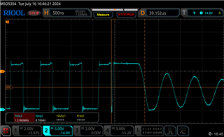
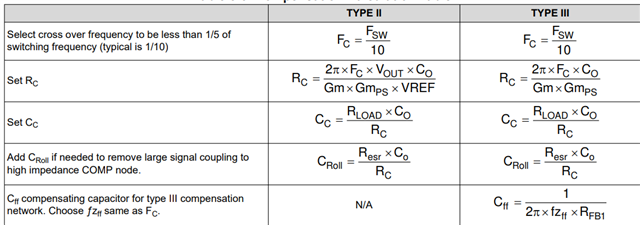
Correct working Vout adìnd Switching:


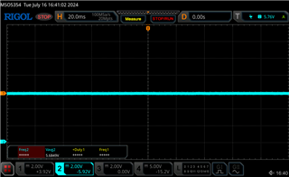
All this tests are made with no load on the regulators output.

Since i dont need to use buck1 and 2 with output current higher then the other bucks, I  tried to set Imax and Gmps to the same values (2.0A max and Isense gain = 5 A/V).

This has made no result. 

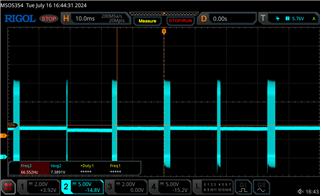
Next I changed the working frequency, Rosc = 120k so 1.49MHz of switching.

Regulator 3 and 4 still working fine and regulator 1 has improved, regulator 2 same problem as before.

Next i changed the values of R933 = 20k ;  C935 = 56nF and C936 = 15p, in order to match the values which work fine with regulator 3 and 4.

Still the problem persists. Is there some other settings i have to use in order to get the 4 bucks to work in the same way?

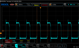
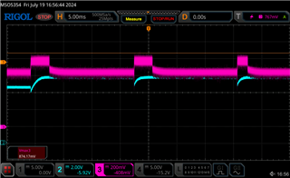
Here the capture of Vout and switching with 48 set as vref in the last test conditions

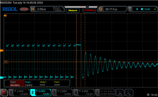
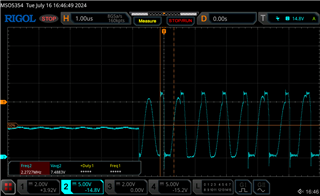
The Vout seems to be stopping every 20ms, this may be related to Output over corrent, but since there is no load I am not sure.

Is there some issue with the setting of the compensation components?

Thank you,

Enrico Bonacini

  • Hi Enrico,

    The schematic image is of really low resolution and I could not figure out the value and circuit. Could you pls help re-upload a high resolution one.

    BTW, could you pls share me some background about the end equipment for example, how TPS6500 is used, like to power for what?

    Thank you!

    BRs

    Lucia

  • Hi Lucia,

    Here is the schematic, hoping this time it is uploaded correctly.

    TPS65400_EB_schematic.pdf

    In out application the 4 output of the TPS65400 will power a device used in printing application.

    Now the output are on an open connector.

    Thank you,

    Enrico Bonacini

  • Hi,

    I have a further question:

    VDDG capacitor should be connected to AGND or PGND? because in pin description it says PGND, but in the other figures it reports AGND.

    Thank you

  • Hi Enrico,

    (1) I just had a quick glance of your schematic and noticed that the inductor is 33uH which is really large and not necessary. 

    (2) Just want to clarify with you, what is input voltage range? And what is your target Fsw, Vout1/Iout, Vout2/Iout2, Vout3/Iout3 and Vout4/Iout4? From the schematic, all four Vout are 7*0.6=4.2V, correct?

    after startup all 4 output voltages are correct with defualt vref (5.6V)

    (3)Do you mean default Vref which is 0.6V? 

    when i change the vref value (to 48 decimal)

    (4) Which Vref do you plan to change to and why?

    in general Ioutmax = 0.3A and Vout = 7...9V.

    (5) Just double confirm, what is your target Vout for all four rails? From the schematic, looks like it's 4.2V.

    Thanks!

    BRs

    Lucia

  • Hi Lucia,

    I reply for point:

    1) I used the formula reported in pag. 56 of datasheet, with ripple current of 0.3 it results 33uH of inductor (more or less), model used ASPI-4030S-330M

    Can you suggest a configuration to test?

    2) Vin is 17.0V (I checked and it's correct), we need to precisely set Vout. 

    At start up all outputs are 7*0.8 = 5.6V (default value of Vref = 0.8V); then with I2C we set each Vref according to the required voltage.

    3) default Vref is 0.8V, 0.6V is the minimum value.

    4) We will read from the device we are going to power it's correct working voltages, typical values will be between 7 and 9.5V, and then set Vref for matching these values. With actual resistor devider we can reach 13V max approx.

    5) typical value between 7 and 9.5V. Here i2c control will always be present.

    I add further informations:

    - We set all channels with same Frequency (freq/1), same Gmps (5A/V) and same Iout max (2A)

    - I thought the inductor was at limit value for the set switching freq (180k resistor => 1.009MHz), so i increased the switching freq to 1.49MHz (120K resistor)

    This seems to improve the behaviour of channel 1.

    - I tried to apply load to regulators 3 and 4 with good results, 9.5V with 16ohm load working fine, changed Vref with different values and the regulator adapts correctly

    - Regulator 1 seems to be working now with increased frequency, but i am not sure that it's stable enough.

    - Regulator 2 only works fine at defualt Vref (0.8V) an with no Load. If a load (just 50mA) is applied than the voltage is completely unregulated.

    If with no load the Vref is increased than the behaviour of the previous image is present. Th switching work just for a few msec and then stops.

    The Status register just report that the channel 2 PGOOD is NOK, but no other bit is flagged (like over voltage, over current or temperature)

    I tried to modify the connection of VDDG capacitor to PGND, nothing changed. What is it's corret connection?

    I tried to modify the comp values, recalculated for 1.4MHz, Rc = 30k , Cc = 22nF , Croll= 10pF and Cff = 10pF. Output still bad.

    Have you got some suggestion for the configuration of the regulator?

    Thank you,

    Enrico Bonacini

  • Hi Enrico,

    Thanks for your feedback. Pls kindly let me check.

    BRs

    Lucia

  • Hi Enrico,

    Pls follow below guidance to debug:

    (1) TPS65400 max recommend voltage is 18V. In your case, typical Vin is 17V which is close to 18V recommend Vin max. I would suggest that you can probe VIN voltage to ensure there is no obvious voltage spike which could cause the Vin voltage to be over spec. 

    (2) Double confirm your target Vout1. Vout2, Vout3, Vout4. From your description, it will be 7~9.5V for each four rails.

    (3) Choose the inductor: Typically, the value of L is chosen to have the ripple current be 0.1× to 0.3× the full-load current. I suspect you use the real load not the full-load current to get the value of the inductor. That might be the reason why you choose a 33uH inductor.

    (4) Compensation circuit

    (5) You can also use Webench tool and it will generate a recommend typical application circuit for you.

    https://www.ti.com/product/TPS65400?keyMatch=TPS65400&tisearch=search-everything&usecase=GPN#design-tools-simulation

    BRs

    Lucia

  • Hi Lucia,

    1) i checked the input rail, at srtat-up Vin max = 17.7 V in many tests. In order to be sure, i lowered Vin to 16.2V

    2) Correct

    3) For the inductor selection I used 0.3A as current and x0.3 for DIL, so DIL in formula = 0.09A; using 17Vin ; 8.4Vout and 1.48MHz i obtain 31 uH => 33uH approx. Using 16.2V it results in 30 uH => 33uH chosen

    Is that correct?

    4) I used the values calculated with Type 3 compensation of SW1 and SW2 in default config (Gmps 10A/V) for SW2: 

    RC = 14kohm => 15kohm ; Cc = 39.99 nF => 39nF ; Croll = 21.42 pF => 22pF ; Cff = 8.9pF => 10pF

    Now with default Vref SW2 it works properly, also with 17 ohm load. But if we increase Vref, also with NO load, the bad regulation is present.

    Here is the Comp node (pink) in bad working (vout light blue):

    Can you explain me this behaviour?

    I tried to change resistor divider in order to get a 7.2V with 0.8Vref (120k; 15k), the result is still the same.

    Vout around 7.0V = instabilty ; Vout = 5.6V good working.

    5) I tried the Webench tool and it reported strange results:

    8625.WBDesign5.pdf

    2mH of inductor is odd... The values for SW3 and SW4 are similar to the one I have here correctly working, but for SW1 and SW2 it makes different calculations, why? Nominally everything is set to be the same.

    SW1 and SW2 needs a different approach in the calculation? Does they have extra stray capacitance respect the other SW?

    Also, what is the correct connection of bypass Capacitor of VDDG?

    I will try get back to old feddback value, (120k 20k) and try type 2 compensation.

    Thank you,

    Enrico Bonacini

  • Hi Enrico,

    I will check your feedback and get back to you by next Monday.

    BRs

    Lucia

  • Hi Enrico,

    For the inductor, you can use full load current which is 4/4/2/2 for Buck1,2,3,4. Don't need to use the actual output current.

    For regulation problem, I am just curious, in theory Vout is set as 5.4V/7.2V. But if read from the waveform, Vout value will be greater than 5.4/7.2V (channel2 2V/div), right? Could you pls help probe Vout, SW in the same waveform? 

    You can first check whether this issue still exist after you change the inductor.

    And BTW, could you pls send me the schematic of high resolution? I tried to download it but looks like it's of low resolution.

    BRs

    Lucia

  • And for the VDDG connection, as you can refer to layout example of TPS65400 User's guide, it shares the same ground with the capacitor which is connected with VDDA and the capacitor which is connected with VDDD.

    BRs

    Lucia

  • Hi Lucia,

    thank you for the feedback. So you think i can use an inductor value of 10uH for example? Since it will increase inductor current ripple, for low load like mine, shouldn't it bring the converter in DCM working?

    Here schematic in high resolution, i hope.

    ikm1800i-2ph_ns23_0-test.pdf

    Regarding Vout regulation, yes in the picture i posted Vout is set to 7.2V but it "losees" regulation and vout start moving.

    In the next hours i will provide more picture. Basically, the switching starts working where Vout has incresing behaviour, and then stop switching as COMP pin falls, al in last picture i send you.

    In my opinion it's a compensation issue, but i cant tell which is the cause. Do you think it will be helpfull to lower slope compensation?

    Ok for VDDG connection.

    Enrico Bonacini

  • Hi Lucia,

    Here I have fixed the output with resistor divider 120k 15k with defualt Vref. With my test i have seen no difference in output behaviour:

    Yellow : COMP ; blue : OUTPUT ; purple : SW

    Vout should be 7.2V but the output "moves" a lot.

    It seems that comp pin "stops" and due to this the switching is blocked.

    What can i do for setting new comp values? Aare there reccomanded maximum values for Rc Cc Croll?

    Thank you,

    Enrico Bonacini

  • Hi,

    i have looked at SS pin of SW2. He never reaches it's stable value, like other regulator do. It's always stopped and restared.

    From datasheet this behaviour seems to be realted to OVP or UVP of feedback pin.

    Are my feedback resistor values to high?

    Thank you,

    Enrico Bonacini

  • Hi again,

    I think now that the problem is that Vfb goes in OVP or UVP, watching the FB pin regulator 2 it is possible to see almost 200mV of oscillation.

    This is present in smaller amplitude also on SW1, but is not present on SW3-4. This noise is creted by the switching of the buck.

    I can watch SS recyclyng eternally without reching its final value.

    The strange thing is that this noise is not present on the output voltage in the upper resistor of the feedback.

    Here blue is output and green is the feedback:

    AC coupled 0.2V/div

    Sorry for the image, but i had to change oscilloscope.

    The noise on the feedback is much higher than the noise on the input of the resistor divider. Can it be created inside the IC?

    Thank you,

    Enrico Bonacini

  • Hi Enrico,

    Pls kindly let me check your questions and give you feedback during these days.

    BRs

    Lucia

  • Hi Lucia,

    Have you got some solutions to provide?

    The problem still persists, the feedback node is too noise and lead to OVP/UVP and to a continuos restart. I tried to put capacitor filter on Vout/Vfb/Vin and Pvin. None of them have worked so far. If i look with oscilloscope the signal are better, less noisy, but ouput still isn't working.

    Is there something I need to change in the internal register configuration?

    If you prefer we can continue by email.

    Thank you,

    Enrico Bonacini

  • Hi Enrico,

    Sorry for late as I am fully occupied these days. But I will try to give you my feedback by today. BTW, could you also send me your layout to review? I would like to double check any noise coupling of fb pin in the layout. 

    Thanks for your understanding.

    BRs

    Lucia

  • Hi Lucia,

    I can send partil layout but I prefer to do it by email.

    I have got un update, we have found a working solution. We have lowered the input voltage to 12.3V, without changing anything more from the schematic I attached in first reply.

    So we have just increased the Duty of the switching node, and now it is correctlyu working, also with load (0.4A) at differente Vref voltages...

    Still the reason for this is missing.

    Have you got a reason?

    Thank you,

    Enrico Bonacini

  • Hi Enrico,

    Could you try with lower switching frequency (for example, change to 600kHz)  when Vin is higher? I would like to verify whether it's related with the limitation of on time.

    Thanks!

    BRs

    Lucia

  • Hi Lucia,

    I had already tried with 834kHz (220k ohm) and the result was bad. The SW1 regulator which was in limit condition has worsened it's behaviour.

    Enrico Bonacini

  • Hi Enrico,

    I will send you a email to review the layout. Thank you.

    BRs

    Lucia