


Other Parts Discussed in Thread: TPS7H1101A-SP, TPS51200, TPS7H3301-SP
Tool/software:
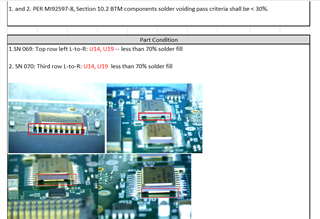
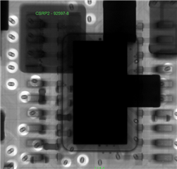
The IPC and J-Standards require a >= 50% solder fill or <= 50% solder voids for bottom terminated components. Some of the components we use we are able to X-Ray the components to see the fill/voiding. However, the way the TI components are construct we cannot get an X-Ray of the solder fill/joint. We just get a solid black picture (see below) due to the construction of the parts. Can we get a process on how to determine the solder fill/voids on these TI parts?
Example parts used:
- TPS50601A-SP Radiation Hardened 3-V to 7-V Input, 6-A Synchronous Buck Converter (attached pictures)
- TPS7H1101A-SP 1.5-V to 7-V Input, 3-A, Radiation-Hardened LDO Regulator
- TPS51200 Sink and Source DDR Termination Regulator
- TPS7H3301-SP Sink and Source Radiation-Hardened 3-A DDR Termination Regulator With Built-In VTTREF Buffer
We have gone to high resolution 3D X-ray and to our vendor Nikon and neither have been able to get results either.
Visual of the TPS50601AHKH/EM part
X-Ray of same area as above
Thak you for your help.

