Tool/software:
Hello,
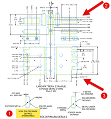
First, on page 2 of RDN0011A, I don't see the dimensions of the copper pads. They seems to be drawn in gray but no quotes.
The pads quoted are in green witch it should be the solder mask opening.
Into the datasheet of the TPSM33615, on page 40, we can see the recommended layout. As a designer, I have trouble to follow
this example because I doubt of that your team spend a lot of time an effort on it. Why?, the PAD #6 is obviously wrong. The design
files of the evaluation board has not routed nets. (BSR236A)
As a designer, we have to choose between IPC recommendations for a package and the manufacturer recommended package.
Must of the time, I follow the IPC standard before the manufacturer recommendations. I use the manufacturer recommendations
when the package is odd and when I trust the manufacturer did a lot of soldering tests with the package. By the quality of what I
see, I am not confident that TI took it seriously enough.
To use it, I would need an updated drawing with a confirmation that you did enough soldering test.
https://www.ti.com/lit/ds/symlink/tpsm33615.pdf
Best regards