This thread has been locked.

If you have a related question, please click the "Ask a related question" button in the top right corner. The newly created question will be automatically linked to this question.

BQ2970: Unexpected potential difference between CELL- and PACK- in normal operation mode

Part Number: BQ2970

Tool/software:

Hello,

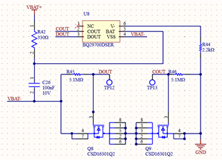
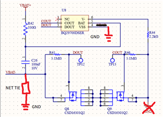
I am following the exact design as the BQ29700 EVM, and even using the same components. Every time the system is powered on (i.e. Cell is connected), I see a voltage difference between PACK- and CELL- for the first time. This causes the actual output voltage to be much lower than the cell voltage. I measure a ~2.7V potential difference between CELL+ and PACK-even when the cell voltage is 3.7V or higher (between CELL+ and CELL-). I am using the BQ29700DSER package. All the hardware components are new and show no signs of physical damage.

When I short CELL- and PACK- together, the voltage differences return to the expected values - i.e. Cell voltage matches pack voltage. This symptom is similar to original author's post.

As a potential mitigation, do you see any issues if a 5Mega Ohm resistor was connected directly between CELL- and PACK- ? Does this bypass the protection circuit instead? I am picturing the case when both FET gates are not driven and CELL- and PACK- have a high impedance path between them. Alternatively, do you have any recommendations to resolve this behavior?

Please see attached application schematic below - 

  • Hello,

    I would not add a 5MΩ between CELL- and PACK-. I think your issue is ground reference placement.

    I would alter your ground placement:

    VBAT- should be your GND reference.

    Best regards,

    Thomas Rainey

  • Hello Thomas,

    Thank you for the A2A. I am not certain if that resolves my problem. I am trying to isolate the CELL- [VBAT-] from PACK- [GND]

    If I connect VBAT- to board GND, doesn't that bypass the BQ2970 entirely? I thought the low-side switching provided a high-impedance return path when the battery voltage did not meet the protection thresholds - i.e. cut off the battery from the circuit. I have components directly connected to VBAT+ and board GND, and if I tie VBAT- (CELL-) and GND (PACK-) nets together, the quiescent power draw of those components will continue to drain the battery even after it drains below the safety thresholds. Also, the design follows the datasheet pin descriptions and example application layout (section 12.2).

    Please let me know if there is an alternative solution.

  • Hello Akshat,

    Sorry I made a mistake. Your original circuit is perfect.

    The difference you were seeing is the discharge circuit not being enabled:

    When the device is first powered it assumes a UVP state. You can follow the instructions above to enabled the discharge circuit.

    Best regards,

    Thomas Rainey

  • Hello Thomas,

    Thanks for the reply and for sharing this caution statement. Could you please link me to the original resource this was obtained from so I can have that as a reference?

    Additionally, do you still see any issues with the 5Mega ohm resistor tying CELL- and PACK-? This should ideally help resolve the discharging circuit issue by bringing both nodes to the same reference voltage on startup. Additionally, the very large resistance value will ensure little to no current flows through when the gates are not driven. Please let me know if there is an issue with this approach and any reasoning as relevant.

    Appreciate the help!

  • Hi Akshat,

    Of course! The caution statement is located in section 9.4.1 Normal Operation of the BQ297xx Cost-Effective Voltage and Current Protection Integrated Circuit for Single-Cell Li-Ion and Li-Polymer Batteries datasheet (Rev. H) data sheet.

    The concern I have is the recovery of UVP and the battery will always be discharging. However, you can test it and see if it works for your application.

    Best regards,

    Thomas Rainey