This thread has been locked.

If you have a related question, please click the "Ask a related question" button in the top right corner. The newly created question will be automatically linked to this question.

TPS22997: Leakage observed on output when load switch is biased (5V on) and ON is asserted (load switch enabled), but input (VIN) is floating

Part Number: TPS22997

Tool/software:

Hello,

My name is Pritam. I am part of the semiconductor group at Google. 

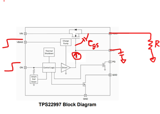
I am using TPS22997 load switch for one of eval board design for essentially creating a power-up sequence.

However, i am observing that when the load switch is biased (VBIAS = 5V is provided) and load switch is enabled (ON pin is HIGH) but with VIN (input) floating, there is leakage on the output.

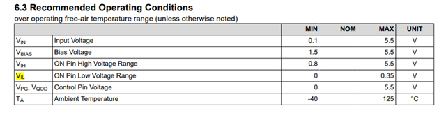
I am providing 5V VBIAS to the BIAS pins. I am asserting the ON pin (HIGH) after VBIAS is provided to the load switch. But, the input pins (VIN pins) are floating...as in there is no input provided to the VIN pins yet.

During this state, i am noticing that the output pins (VOUT) is steadily increasing in level and it keeps increasing until i provide VIN (input pins are no longer floating) or I set ON pin to LOW (or remove VBIAS 5V).

Is this behavior expected of the load switch when the VIN pins are floating (with VBIAS = 5V and ON pin is HIGH)? The databook does not really specify the behavior in this particular situation. I understand that this may not be the intended operation of the TPS22997. But, i am trying to understand if this observation is expected.

And if so, where is this leakage coming from? Is this leakage coming from the VBIAS when VIN is floating (but VBIAS = 5V and ON pin is HIGH)? Thanks.

fyi: i have attached a small snippet of the connections to the load switch. 

  • Hello Pritam,

    Yes, this is an expected observation.

    Since VBIAS=5V and ON pin is high, so FET is in ohmic region. So, a small change in VIN results in drain current to flow and charge the output cap.

    Can you club VIN and ON pin together. So, whenever input gets high only then FET turns ON?

    From snapshot, I can see your VIN is 0.75V. So, you can use ON pin low voltage range using a resistor divider.

    Thanks 

    Amrit 

  • Thanks Amrit. When i am probing the output of the load switch (VCORE_EXT for example in the snippet i shared before), the output cap network is removed from the output. So, input bypass caps are removed. So, there is no output cap to charger. Are you suggesting that the parasitic cap (power plane capacitance) is what's getting charged by the leakage current?

    Also, you mentioned that the pass-fet being in the ohmic region (and that would make the pass fet very sensitive to small changes), a small change in VIN (VIN is floating...no source connected to it) results in drain current to flow. Where is the drain current coming from since (as per the datasheet block diagram) the drain is connected to VIN and VIN is floating? Is there any other place where current might flow into the nmos source (or VOUT) from (like from VBIAS)?

    We can not connect the input to the ON pin because its used for a very specific power-up sequence. And we gate the power to the chip using these load switches and by controlling the ON pin. 

    Thanks,

    Pritam S 

  • Hello Pritam,

    Thank you clearing system condition.

    When ON pin is LOW - VOUT is connected to GND through quick output discharge circuit through a resistance. So VOUT pin is grounded through IC.

    When ON pin is HIGH - quick output discharge circuit is disabled

    What you are seeing on output pin could be the Cgs which is charged by the gate charge pump through output resistor.

    What is the output voltage you are seeing? Can you check with different R value (10Kohms,100Kohms etc) as shown in below image!

    Thank You

    Amrit