Tool/software:
We are using TI’s UCC14140-Q1 Isolated DC/DC Module as a gate drive power supply (GDPSU) in a two-level SiC inverter design. When performing double-pulses tests, the GDPSU output voltage is latching to 0V after both pulses finish when the operating point is at high current. Note that the switching speeds are quite fast in these instances. The GDPSU whose output is disabled is always the high side, and typically occurs when pulses are sent to the low-side (the high-side remains off).
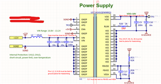
Schematic is seen below. We are using an input of 12V, and an output of 18V. The schematic is based on the reference design in the datasheet.
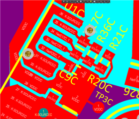
There is an additional 20uF + 100nF capacitance from VDD to K-Source at the gate driver rails.
I believe that the GDPSU is going into a latching fault state. However, if scoped the output rail, and it is not exceeding the over/undervoltage limit, and since it is just a quick pulse, the average power drawn from the GDPSU is low.
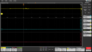
Figure 1: UCC14140-Q1 - CH1: Output Voltage During Switch Transient
After the transient, the voltage is recovered to 18V, but after about 30-50ms, decays to 0.
When I probe the FBVDD pin, I see significant transient. I am thinking this may contribute to this issue.
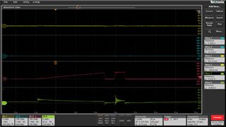
Figure 2: UCC14140-Q1 FBVDD During Switch Transient. CH4 is voltage across C17, CH3 is the current pulse through the SiC FETs.
Can you let me know if there are any other faults that would cause this latch-off behavior that I may have missed? The datasheet recommends a 330pF capacitor across the low-side feedback resistor. Can you suggest any alternative capacitor/resistor values for this pin to reject this noise?
We have done our best to follow the layout guidelines in the datasheet. Our feedback components are not on the other side of the board, but they are close, and there is a single trace to the VDD plane and K-Src pin (35), The plane below it is K-Src.