LMR51420: LMR51420XDDCR

Part Number: LMR51420

Tool/software:

Hello,

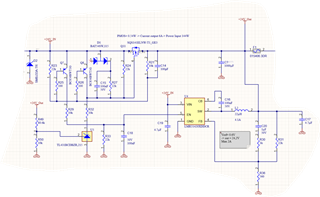
In my schematic, I use the LMR51420 component to precharge my large 1000µF capacitors. My 24V input is switched abruptly by a mechanical switch. When my output voltage becomes close to the input voltage, I disable the LMR51420 and short my 24V in and 24V out with Q11.

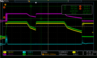
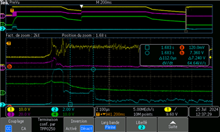
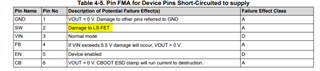
The circuit works well on 30 boards, but I have 5 boards with the U4 component burned out. It burns out quickly during the first three startups. On the functional boards, I have tested with startups, even with a short circuit on the output, and with variations in the input voltage.

I don’t understand why, on some boards, the components burn out, while on others, it’s impossible to destroy them.

Do you have any ideas about this anomaly?

  • Hi Delvar,

    An engineer has been assigned to this and we'll get back to you tomorrow.

    Thanks,

    Andrew

  • Hello Delvar,

    Have you tried an ABA swap to verify whether the issue follows the IC or the PCB assembly? 

    However, your C_FF cap C20 is quite large. The bottom feedback resistor is low. I would suggest ten times the resistance in your feedback network. It's ok for the top resistor to exceed 100k as long as you can keep the feedback trace close to the FB pin and route away from high dI/dT traces like SW or large capacitors. 

    I suspect a high voltage spike from the mechanical switch supplying Vin could affect the Vout/SW net of the DC regulator and cause damage. Can you capture any input/output waveforms for voltage on Vin, Vout, and EN when the switch turns on? 

    Best,

    Ryan

  • Hello, I think the problem comes from the IC.

    I performed tests by removing R50, which leads to a possible activation of Q11 for a voltage below approximately 22V. Additionally, I replaced R29 with 330K (turning on U4 at around 19.6V).

    With the mechanical switch bouncing on the 24Vin voltage, I can quickly damage the U4 component. The same result occurs when removing C20 or adding a diode in series on the output voltage of U4 to prevent current feedback into the component. In this case, the dV/dt at the output can exceed 10V.

    When R50 is connected, the dV/dt is below 2V. This voltage variation is related to the activation of transistor Q11. When R50 is connected, it's much harder to cause damage.

    Here is a recording when the component breaks: Curve 1 (yellow): Vin +24 (behind the on/off switch) Curve 2 (blue): Enable U4 Curve 3: SW U4 Curve 4: Vout +24V

  • Hi Christian,

    I will get back to you shortly.

    -Ryan

  • Hi Christian,

    It looks like the 24V supplied to the output is blowing the IC when input to IC is low. The solution here would be to also stop the voltage applied to output of IC using a switch.

    Regards,

    Rahil