Tool/software:
What are the considerations for using the high-side output of a half-bridge gate driver as a low-side gate driver?
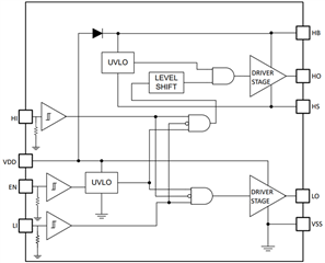
When utilizing a half-bridge driver in a typical half-bridge configuration, an internal level shifter and supporting bootstrapping circuitry is used in order for the high-side output (HO) to be referenced to the switch node (HS) and provide adequate Vgs to turn on the MOSFET. However, when using the high-side output as a low-side driver, the supporting circuitry for the half-bridge is no longer needed. These components include the bootstrap diode (internal or external) and the bootstrap capacitor. When using as a low-side, VDD is adequate to bias both driver outputs due to being 12V typical and referenced to ground. In order to operate the two channels independently, it is best to use a half-bridge gate driver without input interlock. The functional block diagram of the half-bridge driver such as the UCC27311A(-Q1) can be seen below.

Some of our half-bridge gate drivers come with a feature called input interlock that does not allow both HO and LO to be high at the same time if HI and LI are both high. This feature is used to prevent a shoot through condition in a half-bridge circuit. With two low-side circuits and a dual-channel driver or half-bridge setup as discussed above, shoot through is not a concern due to the two-separate low-side circuits. Therefore, a driver without input interlock would be selected unless there was a need where both outputs should not be on at the same time. An example of a half-bridge gate driver without interlock is the UCC27311A(-Q1).
How to modify the typical half-bridge gate driver circuit for dual channel low-side operation?
The most important change to be made is the connection of the HS pin to VSS. This negates the internal level shift so the high-side output is referenced to ground as needed for low-side MOSFET operation. Then, the bootstrap capacitor is not required as the high-side biasing can be done with the VDD capacitor. The bootstrap capacitor that is connected from HB to HS can still be placed and would act as a second local bypass capacitor that would reduce the noise when sourcing current for the HO output. Due to the lack of need for a level shifted high-side, VDD should be connected to HB to provide a good bypass on HB with the VDD capacitor. The connection between HB and VDD negates the need for an external bootstrap diode or bypasses the integrated bootstrap diode. As an example, an interleaved boost PFC circuit is shown below to show how both channels of a half-bridge gate driver like the UCC27311A(-Q1) can be used as a dual channel low-side driver like the UCC27444(-Q1).

Why use a half-bridge driver instead of a dual channel low-side driver?
Some half-bridge gate drivers have a feature that is an enable function to enable/disable the outputs. This enable pin is also typically found on single and dual channel low-side drivers. For dual channel drivers like the UCC27444(-Q1), there are two enable pins so each channel can be shutdown independently. For the half-bridge drivers with enable like the UCC27311A(-Q1), a single enable pin controls both outputs. This could be helpful if there is a need to disable both low-side circuits at one time and would minimize the amount of PWM signals required for enable by the controller.
In the case that high drive current is not needed, a low current, cost effective option for a half-bridge driver is the LM2101. It is a 0.5A source, 0.8A sink current driver that is rated at 107V and can be setup as shown above as a dual channel low-side driver. In addition to being cost effective, it is offered in a small 2x2 DSG package that can help reduce board space, overall system size, and weight.

