This thread has been locked.

If you have a related question, please click the "Ask a related question" button in the top right corner. The newly created question will be automatically linked to this question.

UCC27614: Abnormal work in gate driver.

Part Number: UCC27614

Tool/software:

Dear master.

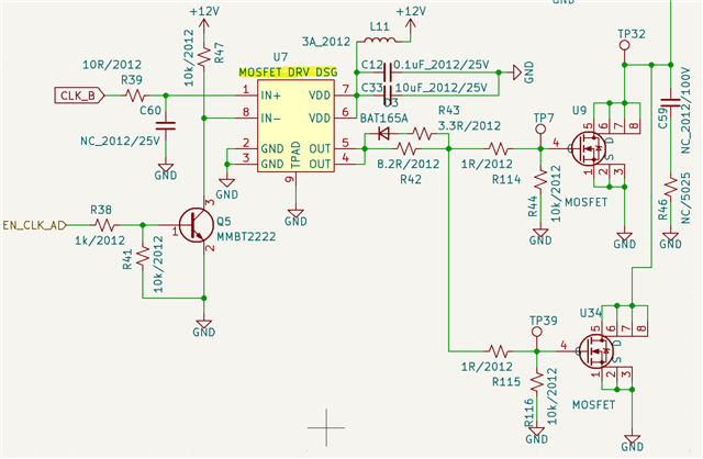
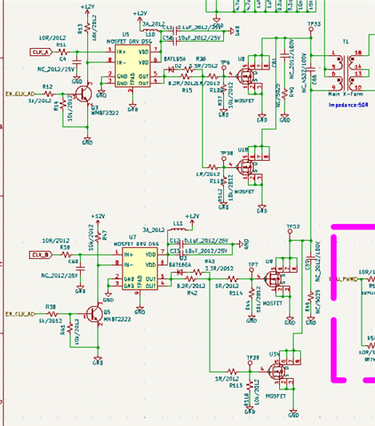
I'm using UCC27614   8pin SON DSG Package.

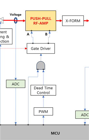
■ UCC27614 Operating Condition.

   - Operating Freq. : 500kHz / 300kHz.

   - FET : BSC146N10LS5 parallel driving.

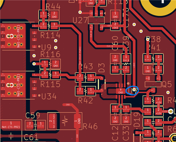
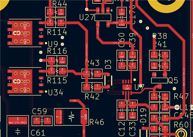
   - Schematic & pattern : See below.

   - 1.6T 2 layer PCB.

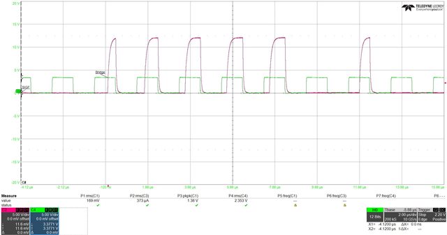
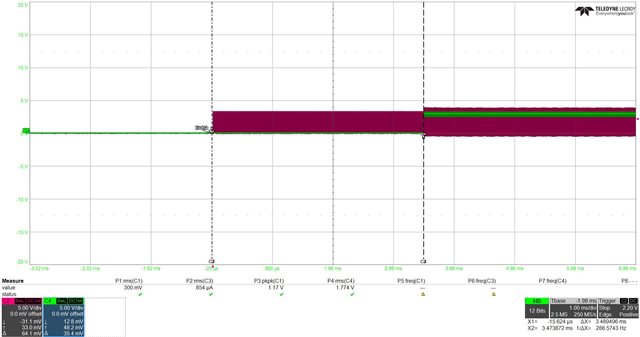
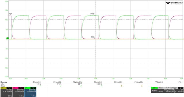
-Trouble : 1 PCB is  out of order. 

                 1 PCB has operating abnormal operation.

Can you advise to me what's wrong?


Schematic

Waveform

Copper PatternPatternThermal Image

IC Marking

  • Hi Sanghyun,

    Thanks for reaching out to TI.

    Overall, the schematic looks mostly okay, but I do have some follow-up questions:

    1. Can you comment on the L11 inductor on the VDD pin connected to pin 6 and 7?
    2. Can you confirm the timing on Clock_A and Clock_B and if they are synced?
    3. Can you send an updated waveforms diagram that contains the following:
      1. IN+
      2. IN-
      3. VDD
      4. OUTPUT

    Thank you!

    Jeremiah

  • Dear Jememiah.

    Thanks for your fast response.

    1)  L11 : MH2029-800Y

    www.mouser.kr/.../mh-777565.pdf

     2) CLK_A, CLK_B is Pushpull type RF-AMP.


    3) CLK_A, CLK_B, EN_CLK_A  signal is controlled by MCU.

      -First.  VDD(+12V) is always on when system turn on.

      - Second. CLK_B is on when user start.

      - Last. EN_CLK_B is HIGH.

    Please see below waveform. 

    ※ C2(Magenta) : CLK

        C4(Green) : Enable.


  • Hi Sanghyun,

    Thanks for your patience over the weekend.

    Taking a second look, there may be a chance the output waveforms are affected by the EN-CLK-A going low, shutting of the output. However, I'd like some more clarification on some points (my apologies for not specific enough requests!):

    1. What the use case is for the L11 inductor on the VDD pin?
    2. Are the Clock_A and EN_CLK_A synced?
    3. Can you send an updated waveforms diagram that contains all the following in one diagram, with a 2us/div (the previous response only has CLK and Enable on a 1ms/div)  :
      1. IN+
      2. IN-
      3. VDD
      4. OUTPUT

    Thanks!

    Jeremiah

  • Dear jeremiah.

    1) L11  Usage :  Prevent spreading EMI from IC.

    2) Clock_A and EN_CLK_A timing.

       - First, Clock_A  is running .

       - Second EN_CLK_A is high after  3.5ms of Clock_A  running.

    3) More detailed waveform will be update next week after our company's summer vacation.

  • Hi Sanghyun,

    Can you try a couple of these design changes:

    1. Removing L11 inductor, since it might affect VDD
    2. Can you change CLK to 5V, in a previous diagram you provided it's at 3.3V

    Additionally, can you comment on when exactly the unexpected behavior starts (at start-up, after a few seconds, etc.) if it's not addressed in the detailed waveform previously requested? 

    Thanks,

    Jeremiah

  • Hi Jeremiah.

    I can also change my schematics as your suggestion  if there is reasonable issue.

    But I want to know why IC is not working well.

    I have 1 question about the IC.

    I am most suspicious of the distance between the 12V output port signal and GND.

    The distance between the 12V signal and GND is only 0.2mm due to the structure of the IC.

    What do you think is the recommended distance for 12V voltage?

  • Hi Jememiah.

    I attached what you wanted waveform.

    1)  FET  gate input signal. (Pushpull A, B)

    FET Gate pin (Push-Pull)

    2)  Signal in, Enable, VDD.

     - C1 : Signal input.

     - C3: VDD (12V)

     - C4 : Signal output.

    Signal in, VDD, Signal out

    3)  Signal Input, Enable, Signal Output

    Signal input, Enable, Signal output.

  • Hi Sanghyun,

    Our expert is out of office today, and he will get back to you by the end of the week.

    Thanks,
    Rubas

  • HI Sanghyun,

    The waveforms you most recently sent look like typical behavior we'd expect from the device. Is this setup that you took the waveforms on performing without failures?

    Something else of note though is there is a lot of noise on the VDD signal on switch. One other recommendation is rotating the C12 and C33 capacitors 90 degrees so they are perpendicular to the device pads, making sure the 0.1uF capacitor (C12) closer to the device.

    Thanks,

    Jeremiah

  • Thanks for your reply.

    I agree  that  there is a lot of noise on VDD.

    But VDD signal always keep over 11Vdc.  I think this noise does not effect wrong operation.

    I have experienced two failues with this IC.

    First time,  IC didn't have any out signal. So I replaced it .

    Second is  abnormal operation as you see above  picture. ( I keep  this wrong operation sample).

     This sample is operating well first time.  I don't know when this situation is occur.

    I have 2 questions.

    1) Clearnce between gate driver output signal to GND.

     - UCC27614 SON DSG is too small package.

       I'm worried about  the clearance from output signal to ground.

    2) Internal logic.

     -  Is there any issues from other person's claim about this IC?

        is there any sequence of  EN/IN- , IN/IN+ pin ?

        As you see above picture,  EN/IN- pin is activated (LOW) after IN/IN+ pin signal(Clock) is applied (eighth picture).

        or Are you check internal logic?

    If this issue's reason is clearance, I will change SOIC package.

    If not, I cannot sure this problems will not happen again. ( I can also change sequence of IN-, IN+)

    I need you and your company's expert groups' help.

    Best regards.

  • Dear Jeremiah.

    Bad news.

    Third NG PCB has happened today.

    Today's bad symptom is that the 12V power on the PCB is dropping, and the cause is the gate driver.

    Please find a quick solution.

    Also, I attached a picture of the IC mark above, so please confirm if it is genuine.

  • Hi Sanghyun,

    For the third issue that you just reported, can you send a waveform and tell us if it's on startup or after some time after startup we're seeing power dropping?

    As for the other questions, the DSG should perform similarly to the D package under normal operating conditions and with good layout.

    The pictures 2 and 3 you send on August 5th seemed not to have anything unusual about them. Can you try some of the noise reducing suggestions and see if the problematic behavior still exists? Additionally, you could try switching to the D package and see if the same failure is occurring with that SOIC package.

    Thanks,

    Jeremiah

  • Dear Jeremiah.

    Third issue is happened several minute late after start.

    I will try to reduce noise reduction, and reply to you.

  • Hi Sanghyun,

    Thanks for some of that info. Please let us know what the results of your findings are and we will discuss further after!

    Thanks,

    Jeremiah