Tool/software:
Hi all!
Let me continue with this thread (cannot continue there, already locked).
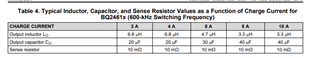
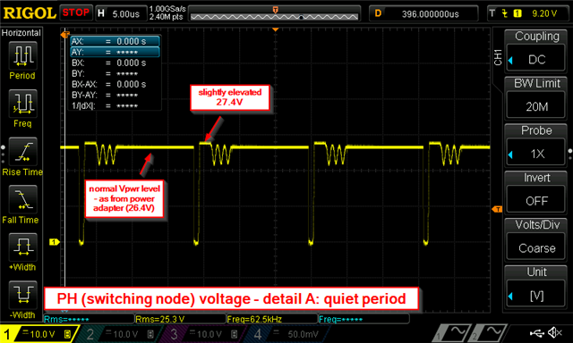
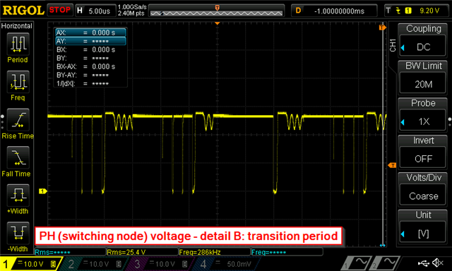
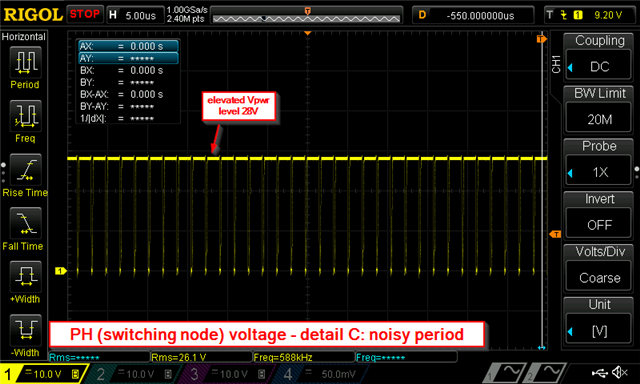
Quick reminder: during end stage of charging ("Fastcharge voltage regulation phase"), when current is ramped down, the output voltage (called "Vpwr" on my desing, or "SYSTEM" in datasheet), experience little bumps from 26.4V to 28V. These bumps last about 0.5ms, and are repeated every 3-5ms. These cause audible effect on input ceramic capacitors (C8, C9 on datasheet fig. 20). What is significant, is that these bumps reach voltage that is higher than input power adapter, and obviously than battery voltage. It means this voltage must have been induced by switching action of charger. I can deal with the noise somehow, but again - is it something that can happen with BQ charger, or should I be worried that it is a symptom of underlying design error.
Let me show you screenshots of PH pin voltage (switching node):
Christian Moyer, you said, related to noisy capacitors issue:
This might be related to the diode on Vpwr, This should be a MOSFET.
I desoldered the diode between Vbat and Vpwr, but the noise is still there. Waveforms are exactly the same. This issue is encountered only during voltage regulation phase. During current regulation, everything seems fine, and PH waveform looks text-book correct.
Does anyone experienced similar problems with QB charger?
Cheers,
Mateusz Karabela