This thread has been locked.

If you have a related question, please click the "Ask a related question" button in the top right corner. The newly created question will be automatically linked to this question.

UCC21750: Failed measurement on isolated side of the digital isolator

Part Number: UCC21750


Tool/software:

Hello all, 

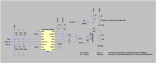
I am trying to simulate the UCC21750 Gate Driver on LTspice. 

I have followed all the recommendations as given in the datasheet regarding the connections on this IC but so far I have not been able to get the model working. The simulation time is extremely long and I am not able to scope any signals. 

I have gone through two other related posts but I did not see any resolution for this issue. 

I have attached a screenshot on my model here.

I would really appreciate any help or recommendation. 

Looking forward to your reply. 

Best regards, 

KKotsis

  • Hi KKotsis,

    Can you try the attached model? It is a difficult part to get right. What features are you most interested in? Could you make due with a model that does not have an APWM pin for example?

    Best regards,

    Sean

    0702.UCC21750.lib

  • Hello,

    The model you shared seems to be working better than the model I downloaded from the website. However, I am still getting a behaviour which I cannot explain and solve. 

    If I only assume one ground (let's say LV_GND) and refer both sides of the IC to that same ground, the gate driver seems to be working fine. You can see this in the picture I have attached. 

    When I try to include a MOSFET and a HV system into the model however, and try to separate the two grounds (so LV GND on the primary side and HV GND on the secondary side of the IC, the driver does not work anymore and the gate pulses in its output look as shown in the figure below: 

    So again, I cannot seem to find where my mistake is or if there is something I am missing with regards to how the connections to the UCC21750 should be. 

    Regarding your question: My intent is to use this IC as a gate driver for a SiC MOSFET Module (will use two of the ICs for High side and Low side) so my main focus is on the gate driver functionality of the IC. 

    Therefore. for now, I can make due with a model that does not have an APWM pin, eventhough I also plan to use this pin on the designed gate driver as well (probably for temp of voltage measurment). 

    Looking forward to hearing from you. 

    Bes regards,

    KKotsis

  • Hi KKotsis,

    I am not sure how the divided ground works here. Can you at least run the Mosfet with low voltage ground on both sides?

    Best regards,

    Sean

  • Hi Sean, 

    I can indeed run the Mosfet with low voltage and having the same GND on both sides. 

    However, for my application I will be working with HV and I would like to replicate the system that I intend to design. 

    Therefore, simulating the system at LV would not really give me any insights. 

    Hopefully there is a way to solve my issue. 

    Best regards, 

    KKotsis

  • Can you drive a half bridge with VSSA at a floating potential? Maybe you only need to short VSSB and GND. That should still give you insights. I don't model cross-channel glitch or anything like that. 

  • Hello Sean,

    I will look into this and post again if I have any questions or results. 

    Best regards,
    KKotsis