This thread has been locked.

If you have a related question, please click the "Ask a related question" button in the top right corner. The newly created question will be automatically linked to this question.

TPS62816-Q1: TPS62816QWRWYRQ1 Jitter question

Part Number: TPS62816-Q1

Tool/software:

Hi TI team,

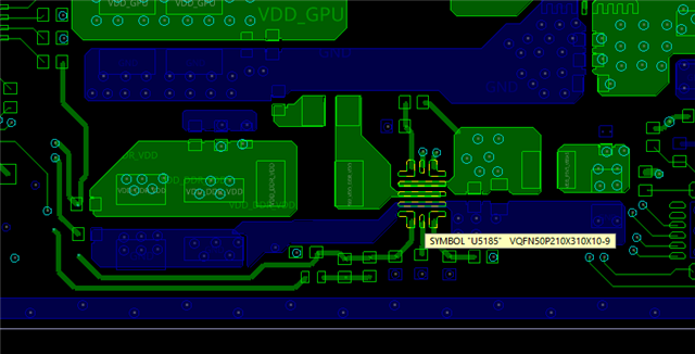
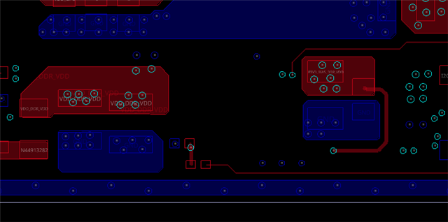
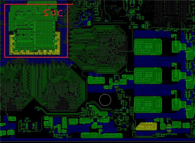
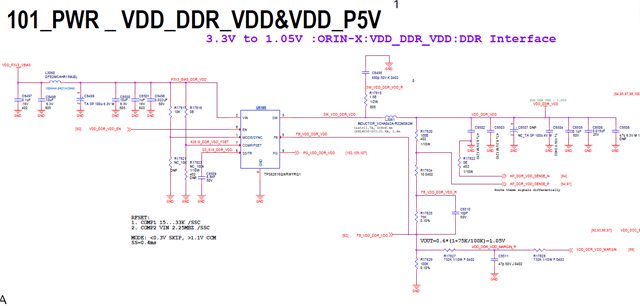
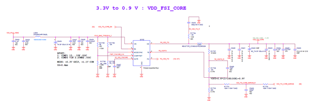
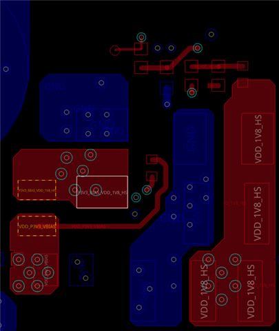
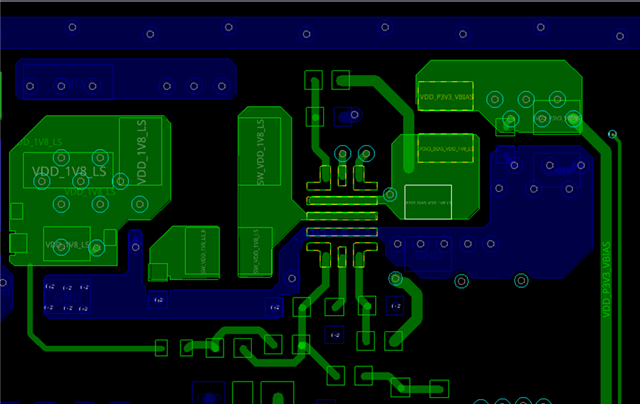
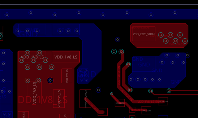
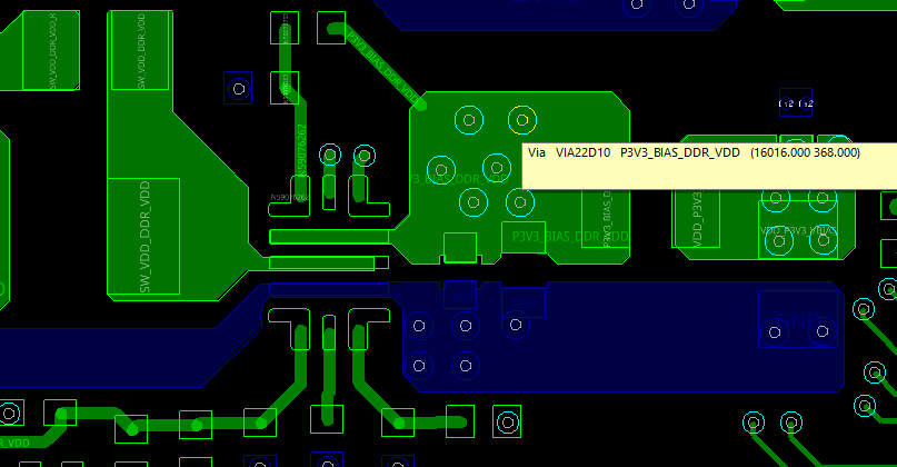
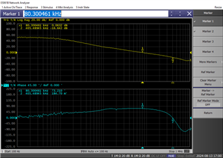
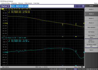
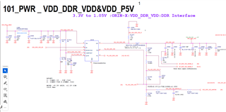
Here is schematic below,
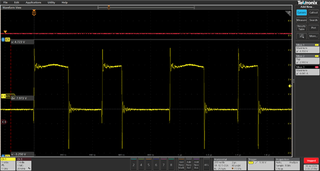
Vin=3.3V

Vout=1.05V

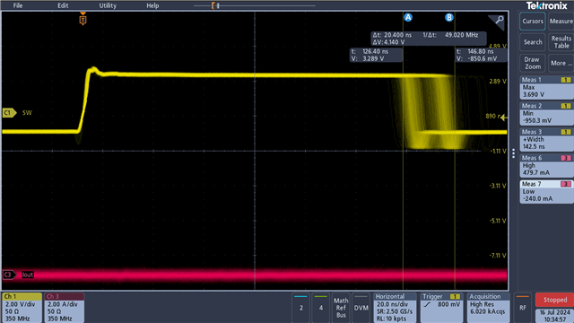
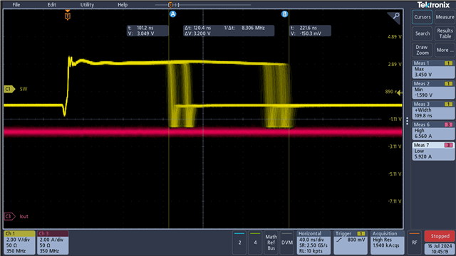
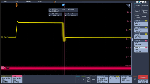
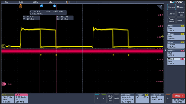
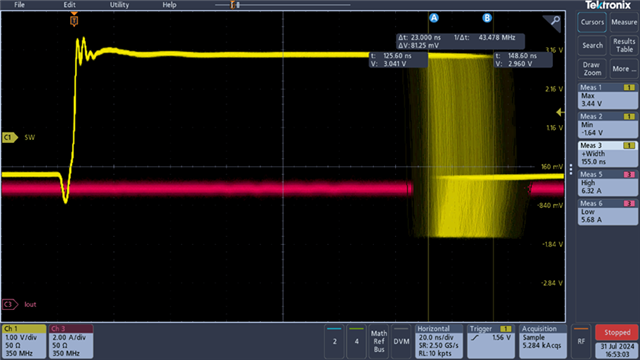
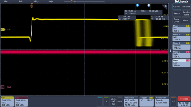
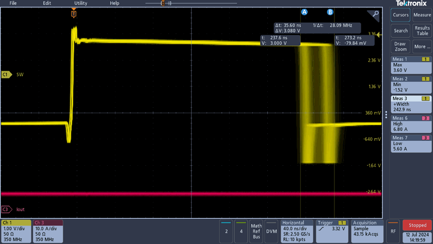
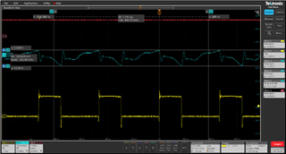
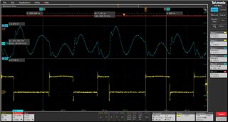
When the loading apply above 4A, the jitter shifts quite large. It looks like not a normal behavior.

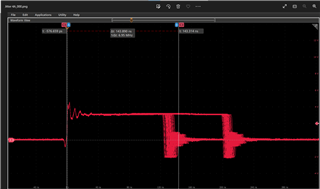
I have checked my downsteam loading, and it is turn-off. Even when SSC is disabled, the phenomenon is still the same. 

Do you have suggestion for this phenomenon? Thanks.

  • Hello Alex,

    Thanks for reaching out to us.

    To verify the issue, can you kindly share the screen shot of the PCB layout? In addition, try to pull to GND the pin 7 (COMP/FSET) by changing R17823 to 0-ohm and removing R17818 and check the duty cycle at Iout > 4A.

    Best regards,

    Excel

  • Hi Excel,

    Thanks for your quick response.

    Here are the result with SSC and without SSC mode.

    1. With SSC, 0A

    2. With SSC, 6A

    3. Without SSC 0A

    4. Without SSC, 6A

    a. The layout TOP veiw.

    b. The layout BOT veiw.

    c. The layout with sink device (SOC removed to make sure no loading)

    Best Regards,

    Alex

  • Hi Alex,

    Thanks for sharing detailed information. Please see my comments below.

    1. The schematic diagram looks fine.

    2. Duty cycle jittering could be due to higher noise on the FB circuit at Iout > 4A load

    3. With SSC enabled, it slightly increase the duty cycle jittering

    4. Possible options to reduce duty cycle variations:

    i. Select a COMP setting 1 (tie COMP/FSET pin to GND) --> check transient response as Comp setting 1 could result to higher output overshoot/undershoot

    ii. Reduce Fsw to 1.8MHz if possible --> could impact the transient response as well

    The duty cycle jittering should NOT be attributed to control loop instability.

    Best regards,

    Excel

  • Hi Excel,

    Thanks for your feedback.

    I have preliminary solution and will update to you soon.

    Best Regards,

    Alex

  • Hello Alex,

    Looking forward for your updates.

    Best regards,

    Excel

  • Hi Excel,

    We found that layout difference on input side results in PWM unbalance issue. 

    Here are 3 different ways to solve the issue:

    1. Removing input inductor(L3060) and short the connection to VDD_P3V3_VBIAS with soldering.
    2. Moving input cap 10uF from Bottom layer to Top layer (Same layer with input inductor and chip)
    3. Connecting external power supply and increasing the input voltage to 5V

    ================================================================================================================= 

    In the original VDD_DDR_VDD status, you can see figure below, the PWM is not stable. The pulse width will go wide and narrow alternately. I tried to add 47uFx3 caps on output side, and the result is no changed.

    Then, we checked with the result in other rails since the jitter behavior is no problem on the other 3 rails with same TPS62816 solution. 

    Now we separate four groups for TPS62816 solution.

              X. U5185_VDD_DDR_VDD

             A. U5182_VDD_FSI_CORE

             B. U5187_VDD_1V8_HS

             C. U5194_VDD_1V8_LS

     Here is the waveform below,

    A0) VDD_FSI_CORE (U5182 with SSC)


    B0) VDD_1V8_HS (U5187 with SSC)

    C0) VDD_1V8_LS (U5194 with SSC)


    From above waveform, the jitter is fine with the SSC mode. So, we tried to compare the difference from schematic and layout.

  • Schematic Comparison

    Gourp X,A,B are almost the same. But on group C( VDD_1V8_LS), the input polymer cap 100uF is populated before input inductor(L3074), and the output cap arrangement is also different. Luckly, the jitter behavior is normal on VDD_1V8_LS.

    X1) VDD_DDR_VDD schematic

    A1) VDD_FSI_CORE schematic

    B1) VDD_1V8_HS schematic

    C1) VDD_1V8_LS schematic


    Layout Comparison

    X2) VDD_DDR_VDD TOP & BOT layer

    MLCC_10uF(C8500 white highlight) locates on the different layer of input inductor(L3060 yellow highlight) and chip(U5185 yellow highlight).


    A2) VDD_FSI_CORE TOP & BOT layer

    MLCC_10uF(C8457 white highlight) is placed on the same layer with input inductor(L3054 yellow highlight) and chip(U5182 yellow highlight).


    B2) VDD_1V8_HS TOP & BOT layer

    MLCC_10uF(C8535 white highlight) is placed on the same layer with chip(U5187 yellow highlight) but different layer with input inductor(L3064 yellow highlight).


    C2) VDD_1V8_LS TOP & BOT layer

    MLCC_10uF(C8619 white highlight) is placed on the same layer with input inductor(L3074 yellow highlight) and chip(U5194 yellow highlight).

    So the input MLCC 10uF is a main point and it should be placed on the same layer with chip. I am not sure is it a phenomenon about LC Resonance?

    Three  different ways solve the issue:

    1. Removing input inductor(L3060) and short the connection to VDD_P3V3_VBIAS with soldering.
    2. Moving input cap 10uF from Bottom layer to Top layer (Same layer with input inductor and chip)
    3. Connecting external power supply and increasing the input voltage to 5V

    Thanks,

    Alex


  • Hello Alex,

    Thanks for the sharing data.

    The 10uF ceramic capacitor on the input ensures it filters the voltage spikes when the high-side FETs turns on and off. Placing it at the bottom layer reduces the filtering capability of the input capacitor due to parasitic resistance and inductance of the vias making the IC unstable. In addition, this input pi-filter could potentially induce LC resonance.

    Always place the ceramic input capacitors on the same layer and as close as possible to the Buck IC.

    Note: Polymer cap could not effectively filter the voltage spikes on the input while the power FETs are switching due to high ESL and ESR. 

    Do you still additional queries?

    Best regards,

    Excel

  • Hi Excel,

    Thanks for your explanation. 

    1. For the placement, that is quite a normal way to place the ceramic capacitors on the back side through vias. Even though the vias is composed of ESL and ESR, we have 6 vias (Size: VIA22D10) on this shape and this effect should be reduced to very low. It is also enabled to handle enough current changes for output 1.05V@6A requirement. I am not sure why the impact is so large for the placement.

    1. It seems that LC resonance of the input side causes instability. Can you suggest the approach by waveform measurement to help us to know the root cause?

    Best Regards,

    Alex

  • Hello Alex,

    Please see my comments below in blue. I hope I was able to address your queries.

    1. For the placement, that is quite a normal way to place the ceramic capacitors on the back side through vias. Even though the vias is composed of ESL and ESR, we have 6 vias (Size: VIA22D10) on this shape and this effect should be reduced to very low. It is also enabled to handle enough current changes for output 1.05V@6A requirement. I am not sure why the impact is so large for the placement. --> It might be it is not so critical in your previous application because the device switching speed is much slower compare with TPS62816-Q1. You can try to measure the voltage spikes on Vin with 10uF on the top and bottom layers. And I expect the Vin waveforms will cleaner with ceramic capacitor is placed near the IC.
    2. It seems that LC resonance of the input side causes instability. Can you suggest the approach by waveform measurement to help us to know the root cause? --> You can perform input impedance measurement to determine if it has resonant peaks that could potential cause duty cycle instability. See app note below for reference.

    link: https://www.omicron-lab.com/fileadmin/assets/Bode_100/ApplicationNotes/Input_Impedance/AppNote_InputImpedance_V1.0.pdf

    Best regards,

    Excel

  • Hello Alex,

    I'm closing this thread now if you don't have further queries. To re-open it, just simply add comment.

    Thank you.

    Best regards,

    Excel

  • Hi Excel,

    Thanks for your help and give us an effiective way to figure out the problem.

    Here is the further analysis,

    Vin Waveform

    The CH2 was added to check the Vin status, and two conditions were compared for different locations of 10uF. As can be seen on Figure 27 for 10uF placed on same layer with chips, Vin pk-pk is 117mV. However, when 10uF was placed on the back side, the Vin pk-pk increased to 309mV shown in Figure 28. Obviously, the Vin waveform was unstable since input capacitor was not able to support in time for loading requirement, and then it led to the duty cycle change.


    Figure 27- 10uF same layer with chip


    Figure 28- 10uF back side of chip

    Bode Plot Analysis

    The feedback compensation can be checked by applying bode plot measurement. As can be seen on Figure 29 and 30. With 6A current load, the 10uF ceramic cap placement is almost no impact for the feedback control loop. So, the internal compensation can handle the Vin change.

    Figure 29- 10uF same layer with chip (GM:-16.6dB, PM:73.2 degree)

    Figure 30- 10uF back side of chip (GM:-16.4dB, PM:74.3 degree)

    Next, I will try to check the input impedence you recommanded. 

    ===================================================================================================

    I also have a question about the Output Cap setting from datasheet description.

    For V / Vout[V], the last paragraph of Figure 10.1.2.2.2 below shows that when the voltage is as low as 0.6V, the minimum output capacitance changes from 32uF to 53uF, which is also mentioned in Table 9-1 32 uF x V / Vout[V].

    Is it correct that the "first V" of V / Vout [V] is a fixed constant 1 V?

    Best regards,

    Alex

  • Hello Alex,

    Thanks for the updates.

    To address your queries on the minimum effective capacitance, the 4th column in Table 9-1 is a formula to calculate for it. See example below for details.

    Formula (RCF = 4.5k to 10k):  32uF·V / Vout

    For Vout = 1.0V:

    32uF·V / 1.0V = 32uF

    For Vout = 0.6V:

    32uF·V / 0.6V = 53.33uF

    I hope I was able to address your questions.

    Best regards,

    Excel

  • Hi Excel,

    Thanks for your quick feedback.

    As my understanding, when the output voltage increases, the output capacitor requires less capacitance, right?

    For example , as output voltage is 3.3V(RCF = 4.5k to 10k), regardless of the ripple and transient characteristics,

    the minimum effective capacitor can be placed 32uF·V / 3.3V = 9.7uF

    Best regards,

    Alex

  • Hi Alex, 

    You're correct. The minimum effective Cout decreases as the Vout goes up. However, this is just to ensure the converter has a stable control loop. 

    To meet the ripple and/or transient load specs, effective Cout could be potentially increase to meet the application requirements.

    Best regards,

    Excel