Tool/software:
Hi Ti experts,
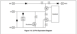
I used bq7695202 to design the schematic diagram of the high-side MOS drive solution. During the test, I found that when there is a voltage input to the PACK (less than the BAT voltage, and this voltage will always exist), the REG1 LDO of the AFE will be abnormally awakened, but this is an abnormal awakening of the AFE working condition, which will cause a power consumption of about 300uA, and eventually consume the battery power.
So I envisioned adding a PMOS to the LD pin to control the LD pin input to prevent the REG1 LDO of the AFE from being awakened when there is an abnormal voltage on the PACK+. The software logic is that when I power on the BMS to initialize the AFE, the control turns on the PMOS and turns the LD pin on to the PACK+; when I shut down the AFE, the control turns off the PMOS. Does this have an impact on turning on and off the DSG? Or do you have a better suggestion? Let me know, thank you.