This thread has been locked.

If you have a related question, please click the "Ask a related question" button in the top right corner. The newly created question will be automatically linked to this question.

TPS73801-SEP: Current Limit vs Input/Output Differential Voltage depending on temperature

Part Number: TPS7H1111-SEP
Other Parts Discussed in Thread: TPS73801-SEP,

Tool/software:

Hello,

My customer was considering TPS73801-SEP for their design. Their requirements are as follows.
Vout = 0.7V to 3.3V
Iout = <1A
Vin – Vout = <0.5V
Ta = -45oC to +85oC
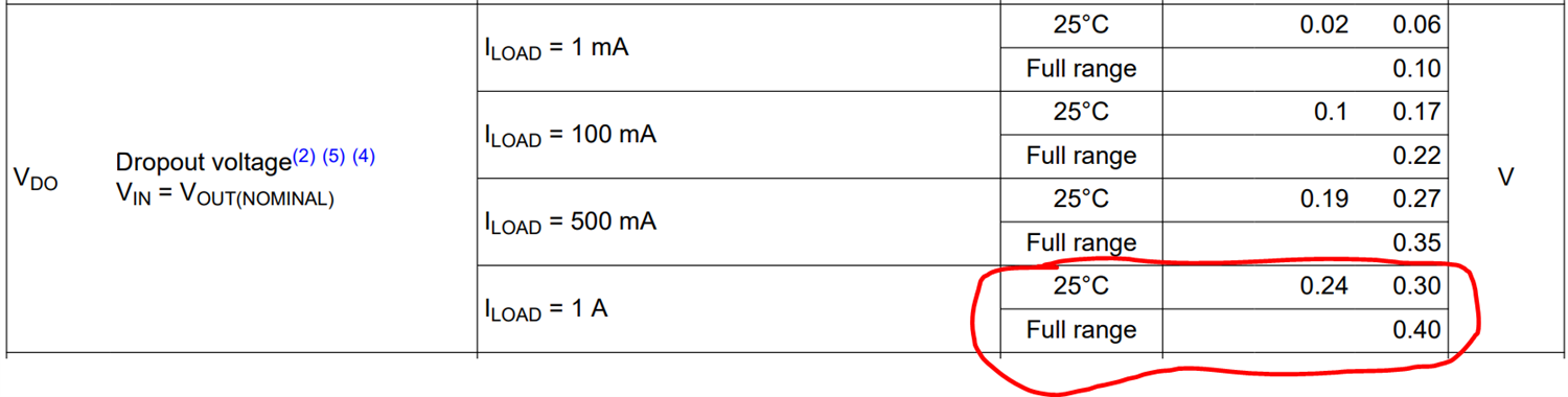
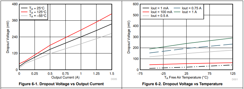
Looking at Figure 6.4 of the TPS73801-SEP datasheet, they are concerned if they could really use TPS73801-SEP at Vin – Vout < 0.5V without triggering the current limit.

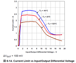
So they also started considering TPS7H1111-SEP instead. However, the TPS7H1111-SEP datasheet does not have plots like the Figure 6.4 of the TPS73801-SEP datasheet. Does TI have plots for Current Limit vs Input/Output Differential Voltage depending on temperature for TPS7H1111-SEP?

Best regards,

K.Hirano

  • Hi Hirano-san,

    In Figure 6-14, there is a test condition at the bottom of the image that states deltaVOUT = 100mV. Basically, in this test VOUT is forced to 100mV below it's programmed value to simulate heavy load across the Input/Output range of the device. 

    Their load is within the rated maximum load for this part (1.5A), so they will not need to worry about current limit during normal operation. This part does not have soft start though, so they may experience current limiting briefly during startup due to inrush current. 

    Since they plan to have a low Vin-Vout differential, they should also be mindful to leave enough headroom to stay above the dropout voltage. 

    The current limit for the TPS7H1111-SEP works differently. It does not vary much based on VIN/VOUT differential and the range of possible VIN/VOUT is smaller. The temperature variation is shown in the electrical characteristics table. The test conditions show that the min/max in each temperature row includes variation from operating across a wide range of VIN.

    Thanks,

    Sarah

  • Sarah,

    Thank you for your response.
    However, I do not understand your explanation about TPS73801-SEP Figure 6-14 well.
    What kind of test was done exactly to get the Figure 6-14 plots?
    For example, at Ta = -40oC, current limit is almost 0A when Input/Output differential voltage is around 0.5V or 0.6V(0.5V +100mV(deltaV)).
    They would like to use TPS73801-SEP at Input/Output differential voltage < 0.5V and Iout =1.0A, but the figure 6-14 shows current limit is around 0A, so they think TPS73801-SEP does not work as expected.
    Am I worng?
    Regarding Figure 6-14, please elaborate more.

    Best regards,

    K.Hirano

  • Hi Hirano-san,

    My understanding is that the testing for Figure 6-14 forced VOUT to be 100mV lower than the value it was programmed for in order to try to pull large load current. The amount of current that the device allowed due the the current limit was then recorded for the range of VIN-VOUT differentials on the a-axis. Unfortunately I do not have the exact test procedure, but that is the general idea.

    During normal operation, a 1A load would not cause VOUT to be pulled 100mV below it's set value so the graph does not exactly apply to nominal operation of the part. The current limit graph is more applicable to startup (when VOUT is much lower than its programmed value & VIN) or to an output fault/short scenario (which the current limit would help protect against).

    I tested a part in the lab to confirm that normal operation with low VIN-VOUT differential would not result in current limiting. With VIN=5.5V, VOUT=5V, and IOUT=1A, the part operates normally. When VIN is lowered to 5.2V the device hits the dropout voltage but output current is not limited. 

    Thanks,

    Sarah

  • Sarah,

    Thank you for your additional explanations.
    But I am sorry I still have concerns that TPS73801-SEP might not meet customer’s requirements.
    Because, looking at the Figure 6-14, current limit is almost 0A when Input/Output Differential Voltage is <0.5V at -45oC. Why VDO could be 100mV under almost 0A load current limit? I do not quite understand this.

    Anyway, can TI officially guarantee that TPS73801-SEP can meet their requirements over all temperature at startup and normal operation?
    Or TPS7H111-SEP would be recommended?

    Best regards,

    K.Hirano

  • Hi Hirano-san,

    Thank you for your patience. I understand that this feature is somewhat vague and confusing.

    Figure 6-14 only applies when VOUT is 100mV below its programmed value, such as during startup or during a heavy load fault condition. The device typically limits current briefly during startup due to the inrush current demanded by the output capacitors since the device doesn’t have soft start.

    However, during steady-state operation after startup (when VOUT is at its programmed value), the device should not limit a 1A load even with low VIN-VOUT differential – this is what I checked in the lab. For this customer’s design, I would only expect current limiting briefly during startup. A 1A load step is unlikely to be strong enough to force VOUT 100mV lower than it’s programmed value and lead to current limiting.

    Regarding your question on dropout at 1mA, typically the dropout voltage is much lower than 100mV but the device does need to maintain some VIN-VOUT differential to ensure it is properly biased to regulate VOUT. 100mV is given as a maximum across temperature and part-to-part variation.

    The TPS7H1111-SEP does have a slightly lower maximum dropout voltage if a separate voltage supply is available to set VBIAS≥VOUT+1.6V (VDO=280mV max @1A). This would give the customer more flexibility with their VIN supply requirements (VIN≥VOUT+VDO). This part also has soft start and a simpler current limit that is easier to understand and guarantee.

    Both parts should work for this design, but the TPS7H1111-SEP would probably be easier to design with and understand.

    Let me know if there is anything you would like more clarification on, or if you have any additional questions.

    Thanks,

    Sarah

  • Sarah,

    Thank you for your additional explanations.

    Q1:
    So, TI can say that the <1A current limit could occur at only startup and never during normal operation?

    Q2:
    Please take a look at the attached powerpoint file, which their understandings about the current limit at startup. Please let them know if their understandings are correct or not.
    Current Limit at startup.pptx

    Best regards,

    K.Hirano

  • Hi Hirano-san,

    Q1: That should be correct. Current limit shouldn't occur during normal steady-state operation. I will check with our designers to see if they can confirm this as well or provide other details.

    Q2: Scenario 1 in their powerpoint may be less likely to hit current limit if the ramp rate of VIN is slow enough to minimize inrush current, such as when the source for VIN has a controlled soft start. Later this week, I can try to provide scopes from the lab to show an example of what each scenario looks like. That will make it easier for me to provide feedback.

    Thanks,

    Sarah

  • Sarah,

    Thank you for taking care of this.
    I look forward to receiving your updates.

    Best regards,

    K.Hirano

  • No problem, I should be able to get to the lab and provide scopes tomorrow.

    Thanks,

    Sarah

  • Hi Hirano-san,

    Here are 4 scopes showing examples of different startup scenarios. Load current was measured on the input side so that inrush could be seen.

    VIN=3.7V, VOUT=3.3V, CIN=1uF, COUT=300uF

    VIN is pink, VOUT is green, Load is blue, and EN is yellow.

    Scenario 1) EN tied to VIN, No Load

    Scenario 2) EN tied to VIN, 1A load (3.3Ohms)

    Scenario 3) Separate 2V EN signal, No Load

    Scenario 4) Separate 2V EN signal, 1A load (3.3Ohms)

    The maximum value of the current limit in my measurements is somewhat higher than the 25C value in Figure 6-14. This could be due to differences in how the tests were performed, part-to-part differences, or differences in the power being dissipated in the part. Overall, the general behavior shown in my measurements is what we would expect though. 

    I hope these scopes clarify the behavior of the part, but please let me know if there are other questions I can help with. 

    Thanks,

    Sarah

  • Sarah,

    Thank you for your response.

    How about Q1, were you able to get confirmation or other details from designers?

    Best regards,

    K.Hirano


  • Hi Hirano-san,

    Regarding Q1: Yes, the device should not limit current during normal operation. Only startup or fault scenarios with high power dissipation conditions will result in current limiting. 

    Thanks,

    Sarah

  • Sarah,

    Thank you for your lab work and confirmation with designers.

    Best regards,

    K.Hirano