This thread has been locked.

If you have a related question, please click the "Ask a related question" button in the top right corner. The newly created question will be automatically linked to this question.

TPS546C20A: I have something with this ic,i want to obtain some support.

Part Number: TPS546C20A
Other Parts Discussed in Thread: USB-TO-GPIO2

Tool/software:

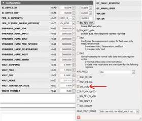
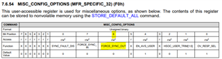
Hi,every one,now i have some issure about tps546c20a,below is describe:

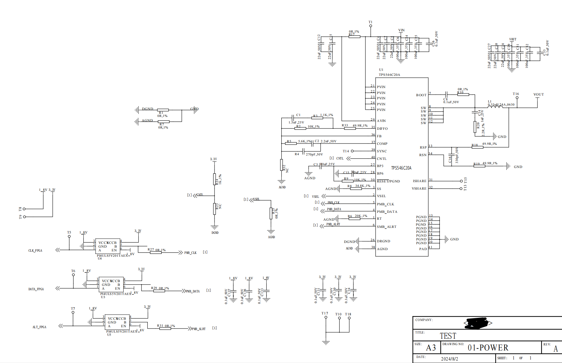
eg: I design a test board of tps546c20a,and the schematic is fully refer to the data manual,but it isn't out voltage,i have some issure.

      1.Is it need config use pmbus that can have voltage out?

      2.Is it can be used alone?

      3.Is there any relevant C language driver code that can be obtained,stm32,and other? 

  •  

    Please share your schematic and operating conditions so we can assist you

          1.Is it need config use pmbus that can have voltage out?

    It depends on the configuration and schematic, but in general the part can be used without PMBus

          2.Is it can be used alone?

    It depends on the configuration and schematic, but in general it can be used without PMBus by selecting the desired output voltage using the pin programming.  Reviewing your schematic would help.

          3.Is there any relevant C language driver code that can be obtained,stm32,and other? 

    TI does not provide a C language driver for the TPS546C20A converter since the functions needed to read and write to the SMBus / I2C controller port of a processor are processor specific, but a standard SMBus/PMBus driver for the specific processor you are using will provide the necessary functions to read and write data via the PMBus commands.

  • Hi,thank you for your reply,this is my schematic.

  •  

    Thank you for the schematic.  A couple of comments:

    1) The TPS546C20A supports the PMBus 1.3 specification, which includes support for termination voltages from 1.62  to 5.5V.  While the level shifters can be used, they are not needed.  The TPS546C20A can communicate directly with the 1.8V CLK, DAT, and ALERT lines.

    2) The existing schematic, with R32 = NC will set the output voltage equal to the internal reference voltage (VOUT_SCALE_LOOP = 1)  and the reference voltage will be set based on the resistor from VSEL to AGND (R25)

    3) With R25 = 0Ω, VOUT_COMMAND (and Vout) will be set to 0.7V.  For other voltage levels check table 2 in section 7.3.7.4 of the datasheet -

     https://www.ti.com/lit/ds/symlink/tps546c20a.pdf#page=18 

    CNTRL is pulled up to 3.3V, so the output will come up to 0.7V with no interaction with the PMBus required.

    If this has resolved your issue, please click "This has resolved my issue" so we can close out the thread.

  • thank you, now i want to know the schematic is ok? i have measured the BP3 and BP6,they are ok,and the cntrl is 3.3V,but the out is 0V,so what should i do to solve the problem?

  • And the sw pin is 0V,boot pin is 0V.

  • Hi,

    There's a few thing that could be going on:

    1. CNTL pin is not setup correctly. By default it's set as active high based on ON_OFF_CONFIG (02h) bit1=1.

    If this bit happens to be changed from default to a 0, then having a pull up resistor to 3.3V wouldn't work. Please double check.

    2. A fault is preventing the output. Look at UV/OV/OC/OT faults. You can look at the specific fault through PMBus (STATUS_....) for more specific or you could also look at RESET/PGD pin which gives a general idea that some fault occured.

    3. Input supply: either not getting enough voltage, or it's fluctuating.

    - What is VIN/VOUT/IOUT conditions you are trying to set for this part?

    - What value are you reading through PMBus for OPERATION (01h) and ON_OFF_CONFIG (02h) commands? are they set as default as shown below:

  • it's sorry to you for reply now,i cann't  get the data to use pmbus,i have not device can supprt the pmbus 1.3,and this value isn't default? they can be changed without any operation?

  • Hi,

    This device can support and is compliant with PMBus 1.3 as mentioned in the datasheet.

    Where you able to get the desired VOUT? and are you able to communicate with the device through PMBus? If no, what are you using to communicate?

    We have USB-TO-GPIO2 (https://www.ti.com/tool/USB-TO-GPIO2) that you can use to communicate to device along with our Fusion GUI downloadable here (https://www.ti.com/tool/FUSION_DIGITAL_POWER_DESIGNER) which will help you read/write to the device. 

    Regards,

    Eileen

  • Hi,it used to the altera fpga(stratix 10 series),the fpga support pmbus 1.3,but it must  the core voltage is ok when the fpga start-up,now the tps546c20a device can have vout without pmbus config? the usb-to-gpio2,i will buy.

  • Hi,

    TPS546C20A device can have VOUT without PMBus configuration by selecting the desired output voltage using the pin programming (VSEL) as shown in table 2 based on your desired VOUT:

    Regards,

    Eileen

  • Hi,now i have a usb-to-gpio2 device,and i can config the tps546c20a in the soft tools,but there have some other problem,as below:

    1.when power up,vin=5v,the vout is ok,that is 0.6v,but when power up,vin=7v(Approximately 7V),the vout is wrong,that is 0v.

    2.when power up,vin=5v,the vout is ok,that is 0.6v,and i adjust the vin=7v,the output is ok, but when i adjust the vin =12v,the output is wrong.

    3.i use the soft tools config the vout=0.9v,and that is ok,but when i store the config to the flash,and power up,the vout is 0.6v still, what? This config is not stored or no use?

    i don't know what's wrong whit this, i really need your help,thank you very much.

  • Hi,

    1) What is VIN/VOUT/IOUT conditions you are trying to set? 

    2) Also, since you are able to communicate with the device now, what are you getting for the status commands below when VOUT=0V?

    3) VOUT_COMMAND does support NVM as shown on table below:

    What is the process you're following to store to flash?

    The correct way would be to use STORE_DEFAULT_ALL [11h] (Send Byte) which copies the entire contents of the operating memory to the corresponding locations in NVM.

    Regards,

    Eileen

  • It looks like there is an extra step to store VOUT to NVM/Flash. The steps are as below:

    1) Set VOUT value through VOUT_COMMAND(21h)

    2) Change OPTIONS(E5h) bit 12: 

    Change bit to a 1 to control VOUT to be managed through PMBus

    This can be done by selecting it through Fusion GUI option as below:

    3) Write byte to STORE_DEFAULT_ALL

    4) Power cycle to confirm change

  • Hi,vin=5v,vout=0.7V,is ok,but i adjust the vin=12V,the vout=0v.,this is the status data,as below:

    cmd  data
    78h   61h
    79h   B861h
    7Ah   F0h
    7Bh   00h
    7Ch   08h
    7Dh   00h
    7Eh   00h
    80h   81h

    the fault has a sync_fault,but the sync is not use,i leave it float, Why is that?

  • Hi,

    Based on the STATUS results provided above you have the following faults:

    OV/UV, OTF bandgap, SYNC, and Low VIN, some which could be a attributed to different reasons, like limits set by commands, device instability, or faults weren't cleared. 

    When you change VIN and/or VOUT, your BOM (fsw, inductor, COUT, etc) has to change in order to support an optimized control loop so it's possible that your BOM wont support all ranges.

    When I do a quick check at 5VIN, 0.7VOUT (where you observe the device regulating properly), based on ton limit calculations, fsw(max)=1000kHz. Your BOM has a Rrt=20k-ohm which corresponds to 1005kHz, which is slightly above but still ok. Now, if I check at 12VIN, 0.7VOUT, then fsw(max)=580kHz, having your BOM with fsw=1005kHz is too high and can cause issues in the device.

    If 12VIN is your desired final input for your design, you will have to change parts of the BOM.

    I can re-check your BOM for stability based on components and tell you what changes need to be made if you provide the final desired VOUT, VIN, IOUT for your design.

    As far as your SYNC fault, I see that you have SYNC connected only to a TP basically floating.  Based on the fault its possible that the device is "expecting an external clock" due to SYNC pin picking up noise through the trace/TP. A sudden change in synchronization clock frequency can cause a control-loop response, resulting in an overshoot or undershoot on the output voltage. To fix this you can try the following:

    - Set FORCE_SYNC_OUT bit(forces the device to output the free-running clock on the SYNC pin). This would be bit 6 of MISC_CONFIG_OPTIONS (MFR_SPECIFIC_32) (F0h) command.

    Regards,

    Eileen

  • Hi,i have changed the schematic as same as the datasheet in 78 pages,but when the vin=12v,the output is error,however,when i change the c14 in sw pin,that is 1nF to 10nF,that output is ok,what's wrong with this?output overshoot?

  •  

    When you say "the output is error" what do you mean?  Can you describe that with a little more detail?

    Would you be able to provide oscillscope waveforms of VOUT and SW so we can help review them?

    Would you be able to provide your layout so we can help review that?

    In your schematic, C14 is a snubber capacitor, which provides energy absorption at the switching node to minimize the resonant ringing of the SW not due to input current build up in the source inductance from PVIN to SW and the parasitic capacitance at the switching node.  If the ringing on the switching node is causing an error in the output voltage, there is likely coupling between the switch node ringing and the remote sense feedback.

  • Hi,i‘m sorry to reply to you now,all of problems is that the pcb layout isn't good, in the new pcb,it is work well,and the snubber C is 1nF,that is the datasheet schematic,and the ic can use to the intel's fpga,i have Verified,finally,thank you for your answer questions.