This thread has been locked.

If you have a related question, please click the "Ask a related question" button in the top right corner. The newly created question will be automatically linked to this question.

BQ76952: IO level; REGIN REG1/2 Dropout

Part Number: BQ76952

Tool/software:

Dear Dear, 

I have two questions:

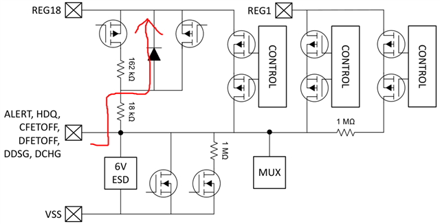
1. If 3.3V level output ports from MCU connect to PINs like CFETOFF/DFETOFF, will high 3.3V level cause leakage through the diode (or MOSFET's parasitic body diode)?
also, If ALERT is cfged as Open Drain output, out side 3.3V pull up resistance will also cause leakage through the diode?
so, the REG18 LDO could be unstable? at least Iq will be increased.

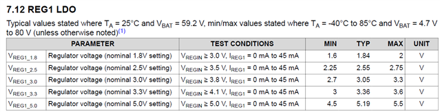
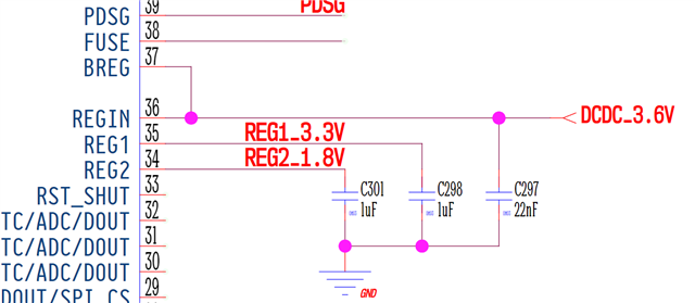
2.  If REG1, REG2 is only configured as 3.3V and 1.8V, the external input 3.6V is OK or not to drive these two LDOs?
REG1 and REG2 wont' be taken too much current, maybe just for level shifting or SPI_MISO output level supply.
There is no voltage drop infos about these LDOs in datasheets.

That's All.

Thanks!

  • Hello James,

    1) If a 3.3V level output port from MCU connects to PINs CFETOFF/DFETOFF, there should not be leakage through the diode or the MOSFET’s parasitic body diode. This is the same with the ALERT PIN if it is configured as an Open Drain output with a pull up resistance to 3.3V.

    2) If the external input is only 3.6V at REGIN to drive REG1 and REG2, you will not get the voltages you desire at REG1 and REG2. Section 7.12 REG1 LDO and Section 7.13 REG2 LDO on the datasheet (BQ76952 Datasheet), can help provide the parameters needed for you to regulate to the desired voltage.

    Best Regards,

    Alexis

  • Thanks Alexis,

    1) So, the diagram in sluaaf2.Pin.Equivalent.pdf is not entirely accurate to reality, right?

    2) Section 7.12 REG1 LDO and Section 7.13 REG2 LDO

    Seems the output range is apparently large,  although it's based on full temperature range. It still can not tell the minimum VREGIN for 3.3V output with IREG close to zero.  Anyway I will try to test on board. In fact, in my case, REG1 3.3V is only to supply SPI_MISO output stage.

  • Hello James,

    1) Yes, the equivalent diagram is not exactly what is inside the part. It is a simplified representation of it to both protect the proprietary nature of the internal design and make it easier to read and understand.

    2) Additionally, the LDO range is also across the full temperature range AND all load conditions (0~45mA). 

    Best Regards,
    Alexis

  • This resolved my issue.

    Thanks for you help.