Part Number: TPS25762Q1EVM
Tool/software:
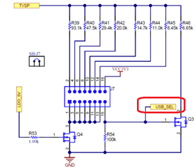
TVSP pin connects to gnd through 6.65k resistor for TVSP index 8 to update FW from USB. Why does the gate of Q3 tie to VCC3V3 instead of LDO_5V like the other options (index 1-7)? Is the timing requirement of TVSP pin for USB update (index 8) different from the other boot options (index 1-7) ?
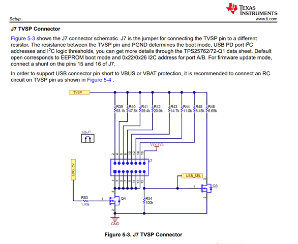
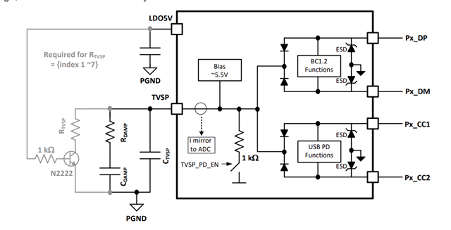
In the datasheet it shows USB update being triggered with a transistor which has a gate tied to LDO_5V, but it also mentions a boot cycle is required.

The datasheet also has a note which says 'required for index 1-7' on the previous diagram. This seems to imply there is something different about index 8.