This thread has been locked.

If you have a related question, please click the "Ask a related question" button in the top right corner. The newly created question will be automatically linked to this question.

LP2951-Q1: Add an external pull-up resistor at Shutdown PIN. Dose it works to shut down the deceive. What are the values of the pull-up resistor

Part Number: LP2951-Q1
Other Parts Discussed in Thread: LP2951

Tool/software:

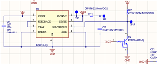
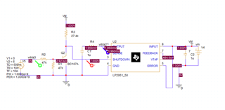
If the shutdown pin is in high voltage state when VDDA2 is disabled. Will the circuits work? See the figure below:
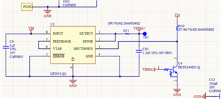
  • Hi Aman,

    Please describe what functionality you are trying to achieve and how you want to implement shutdown of the device. The device will not start up in the configuration you have shown here. The shutdown implementation is redundant and will not work as desired if VM is a fixed voltage that instantaneously switches ON and OFF. Presence of VM will cause leakage current to flow into SHUTDOWN at startup and it will be pulled HIGH before VDDA2 can ramp up and enable U4. So device will be in shutdown mode throughout.

    Do not ground the ERROR pin since it is active low. If not used, it can be left open.

  • Hi Ishaan:

    I want to achieve the functionality is that Using VDDA to control the shutdown for save power consumption. As you say VM is a fixed voltage that instantaneously switches ON and OFF.  VDDA is the LDO 5V output voltage of SOC. LP2951 should be shut down after disable the VDDA and LP2951 is in active status after VDDA return to 5V

    By the way, the configuration of ERROR PIN is connected to ground refers to the following LINK:

    LP2951-Q1: Unused open-collector ERROR pin - Configuration

    Can this work?

  • The circuit as you have it here, will not start. The LGO will not power up because SHUTDOWN would be ON from the beginning itself. Also, why do you want to control SHUTDOWN from output? If the device is disabled, there will be no output and you will not need to shut it down anyway. This is what I meant by the scheme being redundant.

    I apologize for my direction on the ERROR pin. You may ground it.

  • HI, Ishaan:

    Thank you for your patience. I made a mistake in the picture; the net name for transistor base is VDDA3, not VDDA2. See the figure below:

    And I have simulated this circuits in PSpice, it seems work. Could you please check this. The result following below:

  • Hi Aman,

    It looks like you are using VDDA3 to control the shutdown which makes sense now. The scopeshot shows that VDDA3 is usually LOW and assuming VM is always HIGH, so the device is normally shutdown. When VDDA3 rises above the threshold voltage of the BJT, the SHUTDOWN pin goes low and the device turns ON. Please confirm my understanding of your operation and if this is exactly what you desire. 

    Where is VDDA3 coming from? Also, what is the end use/ application of this circuit?