This thread has been locked.

If you have a related question, please click the "Ask a related question" button in the top right corner. The newly created question will be automatically linked to this question.

LMG1210: Disruption of the HO terminal waveform

Part Number: LMG1210

Tool/software:

Hi all,

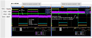
The waveform of HO pin is disturbed, so please tell me the cause and the countermeasure.

HO pn: points in red

LO pin: points in blue

are measurement points.

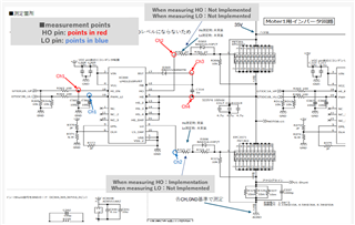
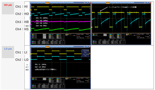
There is no problem with the LO pin,

but the HO pin waveform is distorted even when it is not connected to the FET.

Please tell me the cause and the countermeasure.

If there is information you want, we will measure it and provide it.

Best Regards,

Ryusuke

  • Hi all,

    When a current is applied to the FET, only the HB and HO voltages change. The voltage rating between HB and HS is also 5.5V or more.

    What causes the HB and HO voltages to change?

    If the voltage exceeds the rating, are there any measures such as installing a Zener diode?

    When a current is applied to FETn, the gate voltage and HB fluctuate.

    HB-HS exceeds the rated voltage of 5.5 V, exceeding by about 1 V.

    Best Regards,

    Ryusuke

  • Hello Ryusuke,

    The bootstrap capacitor C314 might be too large and is not fully charged when HO switches high. 

    Please refer to this Application Note for how to calculate that value as well as the VDD capacitor value.

    Bootstrap Circuitry Selection for Half-Bridge Configurations

    Make sure the distance between the gate drive and FETs are minimized. Increasing the distance between gate driver and the power switch will increase the parasitic and may increase the ringing beyond the spec of the gate driver pin. This may cause the damage. The GaN gate driver and the GaN FETs are very sensitive to the gate voltage. A zener diode can also be used to clamp the voltage

    Also, a power supply is not needed for both VIN and VCC/VDD due to the internal LDO.

    Thanks,

    Walter

  • Hi Walter,

    1) The bootstrap capacitor C314 might be too large and is not fully charged when HO switches high.

    →Sends the waveform when the capacity value of the bootstrap capacitor is changed.

    The rated voltage of HB-HS is over 5.5V.

    2) The GaN gate driver and the GaN FETs are very sensitive to the gate voltage. A zener diode can also be used to clamp the voltage

    →In Section 9.3 DON’T4. of the datasheet, it is stated that the GND of the controller (CPU) and the gate driver should be separated.

    Please tell me the reason.

    Also, a power supply is not needed for both VIN and VCC/VDD due to the internal LDO.

    →If the Vin and Vcc inputs are common, should they be separated?

    Best Regards,

    Ryusuke

  • Hello Ryusuke,

    Ringing on HS could be causing the boot strap capacitor to overcharge. Adding Zener clamp diodes and keeping the FETs close to the driver should help.

    Choosing a bootstrap diode with a larger VF might help keep the boot strap capacitor from overcharging.

    The datasheet says to use a common ground between the controller and driver. If the controller and driver grounds are separate there can be a ground reference offset which can cause errors.

    The Vin and VCC pins are not common. There is an internal LDO so a VCC connection is not needed if Vin is supplied from 6V-18V. If a stable 5V supply is available, Vin can be disconnected and 5V connected to VDD.

    Thanks,

    Walter