This thread has been locked.

If you have a related question, please click the "Ask a related question" button in the top right corner. The newly created question will be automatically linked to this question.

UCC21521: gate driver getting failed during start-up condition

Part Number: UCC21521
Other Parts Discussed in Thread: UCC21550, UCC21520, UCC21551

Tool/software:

Hi,

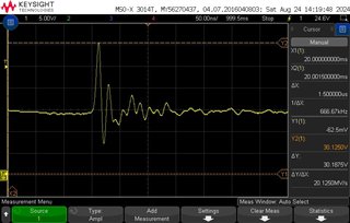
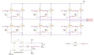
I'm using one gate driver signal to drive two FETs in parallel to manage current requirement of Motor in H-bridge Configuration (<75A).

But, UCC21521 driver failure observed when gate driver fed with VCC Input (3.3V). In specific, failure happens on low-side gate driver section.

Schematic was attached for your reference.

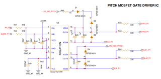
Gate driver design requirements 

Power transistor  - NVHL027N65S3F

VCC - 5.0 V

VDD - 15 V

Input signal amplitude 3.3 V

Switching frequency (fs) -20 kHz

DC link voltage -150 V

I'm quite unclear about failure root cause .To Counter the Issue, I need your expertise on the same.  

  • Hi GP,

    Can you please use the UCC21550 instead? We resolved a lot of issues based on UCC21520 feedback in the updated design.

    The output stage of the UCC21520 is too fast and it can interrupt Igate fast enough to cause Vdd >30V abs max, due to the Vgs loop inductance.

    That is the root cause of a lot of failures. It is not possible in the UCC21551, which has two parallel protection circuits against this issue. Also, more quality controls are added in the the wafer production process of UCC21551 (Over Voltage Stress Test) to eliminate units with weak spots in their large oxide layers.

    Is it possible to use our updated device instead? 

    Best regards,

    Sean 

  • Hi Sean,

    Thanks for your response.

    Does UCC21550 form, fit, function remains same as UCC21521??. if yes, i can test it in parallel.

    Meanwhile, Does any modification in the gate driver schematic will help to counter the current issue??

    Introducing optimum gate resistor to slow down Igate ramp up or soft start capacitor to slow down the dv/dt rise ??

    If we add Protection circuits externally, does it help ??

    Kindly advise..

  • Yes it is a drop in replacement. 

    You can always slow the switching speed, but that will decrease the switching efficiency. You could try a 15V TVS diode across the supply, but it might not be close enough to the voltage spikes to prevent damage. It is worth a try if you cannot use the revised device.

    Best regards,

    Sean

  • Hi sean,

    Thanks for your advise.

    We tried TVS diode SMBJ15A-E3/52 (Stand off Voltage 15V) across Mosfet driver UCC21521 power supply voltage (VDD15V) to clamp the transient voltage that goes beyond 25V.

    As expected, TVS diode clamps fast transients if its crosses 25V and above. But, we still unable to avoid UCC21521 failure which happens on random manner. 

    We replaced UCC21521 with UCC21551 as potential frontrunner. But, Still failure persists on Low side power supply section(short condition exists b/w VDDB and VSSB) even with TVS diode across power supply lines.


      once again, Need your inputs on the same for trouble shooting the issue.


  • Hi GP,

    The UCC21551 failed with the TVS diode? This is a very robust part. There might be something wrong with the circuit itself. Usually these issues come down to high voltage switch node ringing, and the solution is better high-voltage decoupling.

    Does the supply short failure occur on the low-side of the same phase as before? Do you have a measurement of the supply and Vout at the same time? Can you also measure the 150V switch node?

    Best regards,

    Sean

  • Hi sean,

    As you mentioned, High voltage switch node ringing at mosfet turnoff could be the potential cause.

    Does adding Passive Snubber circuit (Series RC network)  across Mosfet drain source will help to bringdown switch node ringing frequency to accepted margin ??

    I would like to brief the Mosfet driver failure scenario to narrow down the potential cause.

    1. BLDC Motor operation is 2-Quadrant (Forward & reverse) with PI close-loop control 

        V_Drive: 100V to 150V &  I_Drive: 75A (Max)

    For Motor forward (Clock-wise) motion control, following are the inputs to Mosfet driver

    > Mosfet driver INA voltage : 0 V--> 5 V (Low to high transition with 100% duty) for High side driver output drive with Vdd=15.

                             INB voltage : 0 V--> 5 V (Low to high transition with 50%~100% duty @20Khz) for Low side driver output drive with Vdd=15.

                             Dead time : 3.6uS

    For Reverse (Counter clock-wise) motion control,        

    > Mosfet driver INA voltage : 0 V--> 5 V (Low to high transition with 50%~100% duty @20Khz) for High side driver output drive with Vdd=15.

                             INB voltage : 0 V--> 5 V (Low to high transition with 100% duty) for Low side driver output drive with Vdd=15.

    when Control system is online, BLDC Motor can be operated either forward or reverse direction w.r.to direction input (5V --> Clockwise & 0V--> counter clockwise) 

    Consider Mosfet driver actuates Motor in Forward direction w.r.t direction input (5V --> Clockwise), Mosfet driver low side failure occurs if we change motor direction from forward to reverse by Changing direction input.

    Kindly advise your feedback on the same..                                

  • Hi GP,

    You can add the snubber across the HV BUS itself, since the switch node will be shorted to either V+ or V- when it is ringing. That means the snubber capacitor doesn't not have to charge and discharge every switching cycle. Also, there is a lot of power there to snub. Normal resistors will burn up. I have successfully used electrolytic capacitors with ESR as RC snubbers, and their large package is able to handle the snubber dissipation. It might be worth a try.

    You can also try different FETs. Higher Rdson FETs usually have lower capacitance, which is one key factor of the switch node ringing. Too large of FETs sometimes can also lead to problems with Miller injection and shoot through. You should right-size the FET's Rdson and Id rating, if you have not done so already and are using a very low Rdson FET.

    Getting rid of switch node ringing is for me an iterative process based on layout. It sometimes takes a while to balance the Ldrain, Cswitch_node, and RC snubber (electrolytic loss tangent) just right for a given design. The fine tuning of the layout is more of an art than a science.

    Best regards,

    Sean