Tool/software:
Hi Team, we are using TPS62932DRLR regulator in our design. We have noticed that DCDC does not work properly in some cases, particularly once the power supply is given the DCDC starts to get hot and propably damaged. We have 3 cases of failure over 50 units, so we need to understand what's going on before next batch of production.
The normal operating situation is:
- Power Supply: 8-30V (extended case), 10-28V (normal case)
- Iout Max: 500mA
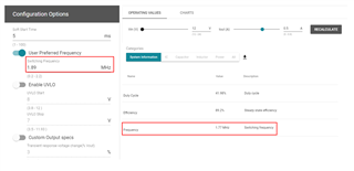
- Fsw: 1.2MHz
- Operating Temperature: -20°C to 60°C
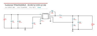
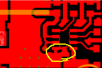
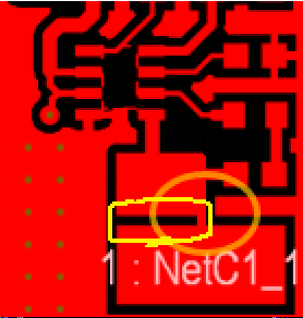
We developed our solution based on the Typical Application Schematic of the "TPS62932DRLR" IC. Below our actual situation:

Here you can find the BOM:
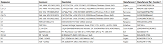
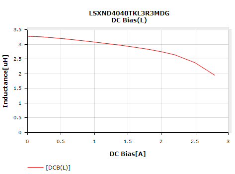
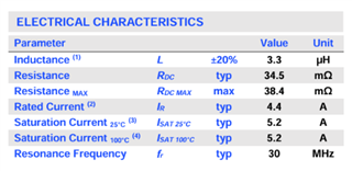
Regarding the inductor, the main parameters are listed below:
|
Type
|
Wirewound
|
|
|
Material - Core
|
|
|
|
Inductance
|
3.3 µH
|
|
|
Tolerance
|
±20%
|
|
|
Current Rating (Amps)
|
|
|
|
Current - Saturation (Isat)
|
2.3A
|
|
|
Shielding
|
Shielded
|
|
|
DC Resistance (DCR)
|
66mOhm Max
|
|
|
Size / Dimension
|
0.157" L x 0.157" W (4.00mm x 4.00mm)
|
|
|
Height - Seated (Max)
|
0.071" (1.80mm)
|
As mentioned before in some cases (only 3 devices upon 50 analyzed until now) we noticed that, once the power has been applied, the circuit got damaged with turning too hot.
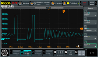
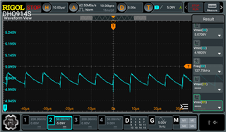
We have done some measurement of the load current profile without the DCDC enabled.
The load current profiles first in normal situation (Iavg = 120mA, Imax = 312mA) and then during the maximum load (Iavg = 380mA, Imax = 550mA) are reported below:![]()
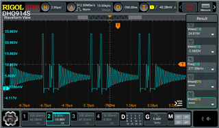
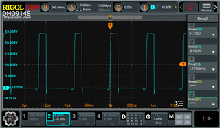
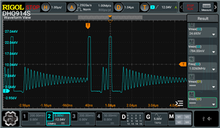
The most critical situation is when the load is connected suddenly by hot plugging. You can see below the load current spike of 1.03A: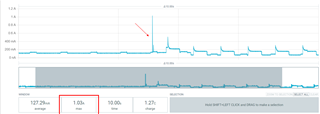
Based on the previous information, we would like to ask you the following:
- Can this configuration and load profile cause oscillations on the DCDC output, consequentially cause instability and damaged the circuit? Can this problem if confirmed eventually affected the MTBF? If so, what would you suggest as component tuning without modifing the PCB (only footprint compatible component replacement) to improve stability and reduce MTBF, even by reducing the operative voltage to 18-28V if required (we can accept this limitation for now)? This power supply IC is intended for a SIL2 product, so we have to be sured about reliability and log term stability. Actually our limitations are the size of the inductor (4x4mm) and that we cannot insert the stability capacitor (Cff). We have already have 500 PCB ready to go in SMD line.
- Thinking about a future more aggresive revision we can modify the BOM adding the Cff capacitor and moving the inductor to a 5x5mm footprint. This is a revision that we can do after the 500 PCB batch.
- One last question, we tried using your tool "WEBENCH Power Designer" and it recommends using an inductor with Isat of 6.3A with a max Iout of 1A. We were expecting a solution with Isat = 2A MAX. Why does your tool recommend this saturation current even if the maximum current set for simulation is 1A?
Thanks and best regards,
Roberto