Tool/software:
Hi.
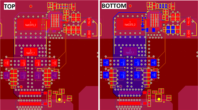
Im designing 30A 0,85V buck converter with TPS548D22RVFR. I want to ask about switch-coil PCB trace. PCB is 1oz copper, and connection between coil and switch is about 200mil wide - should, or can i use second layer (PCB has 16 layers, second layer is GND) to improve this connection current carrying capacity? This connection should be short and small area as possible, so i think i shouldnt use thru PCB vias, so i would use microVias. I know that they can provide smaller current than drilled vias. From the other side i think that using two layers can change nothing, but the heat amount will be the same. I dont want to use bottom layer because i think this will significantli incerase EMI. Can You say couple of words about layout corectness? Cutting GND plane on top layer under coil improves performane?
Below i show my actual layout. Big capacitors on output has 180uF. Two thin traces on the right side are feedback on layer 3.