This thread has been locked.

If you have a related question, please click the "Ask a related question" button in the top right corner. The newly created question will be automatically linked to this question.

TPS62870: VOSNS AND GOSNS

Part Number: TPS62870
Other Parts Discussed in Thread: TPS62873-Q1

Tool/software:

Hi team:

We are currently using TPS6287x-Q1 family for DDR power suuply. I have two questions about VOSNS and GOSNS

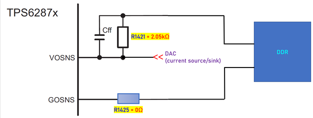
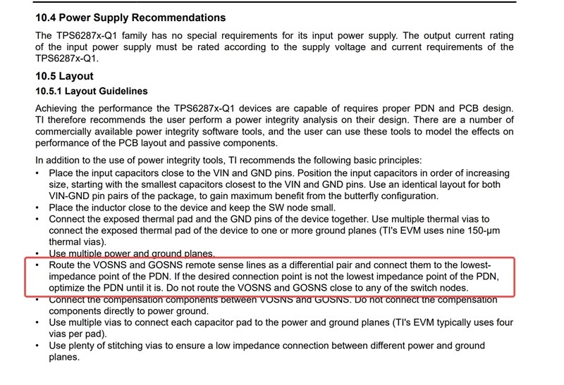
1. From datasheet, it suggests to route this two lines as a differential pair remotely, but I saw an application note, Remote sensing for power supplies (ti.com), Rsns is located remotely, and the other signal is connected to GND locally close to BUCK. From the notec, it seems differential pair is required if the chip equipped with a differential amplifier for remote sensing, but TPS6287x-Q1 family uses just Op amplifier from it's Functional Block Diagram.

My question is, do we need to connect GOSNS remotely from load, or can we just connect it to local GND near buck regarding this TPS6287x-Q1 family, and why is this datasheet layout guidance inconsistent with the application note.

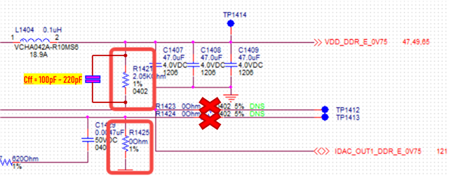
2. Does it matter if we use a 2kohm Rsns to VOSNS, and 0ohm to GOSNS? Since we need this resistor for voltage adjustment, I suppose the resistance of RSNS is not a issue if it's just a Op amplifier inside the chip.

  • Hello cao,

    1. Please follow the recommendations of the datasheet and use a differential pair to the lowest-impedance point of the PDN.

    2. TPS62870 does not require any resistors in its VOSNS and GOSNS lines, as shown in the datasheet section 10.2 Typical Application and the EVM schematics (R12 is only present to enable bode plot measurements).

    Please let me know, if you have any follow up questions.

    Regards, Werner

  • Hi Werner:

    For the resistor, we need a 2k resistor for adjusting output voltage by current DACs, does this resistor affect the performance of voltage sensing?

  • Hi Cao,

    for adjusting the output voltage, please see this app note: https://www.ti.com/lit/an/slvafe6/slvafe6.pdf

    Regards, Werner

  • hi Werner:

    We are using another Sink/Source Current DAC chip DS4424N+T&R to adjust output voltage,and this 2.05kohm is set according to this DAC chip, I wanna ask if this 2.05kohm series resistor affects the differential pair of sensing signals.

  • Hello Cao,

    I just assigned this topic to a colleague with more in-depth knowledge in this topic.

    Regards, Werner

  • Hello Lelian,

    Please allow to jump-in to the discussion. 

    Before I go respond to your queries, I just want clarify few items below.

    1. The I2C feature of the device is being used in your circuit which could be utilized in adjusting the output voltage. Why do you use an external DAC instead?

    2. What is the potential Vout range in your application?

    Best regards,

    Excel

  • Hi 

    1. We need to slightly change output voltage to test the load's performance within input voltage range of the load, let's say shmoo test, it's for testing chips. It's more convenient for us to use DAC

    2. the range is 0.675V to 0.825V

  • Hello Lelian,

    Thanks for the quick response.

    It seems it's difficult to achieve the Vout range with 0.75V default startup voltage considering the sink/source capability of DAC is limited to 200uA max. Is it still necessary to have I2C for this device? Or non-I2C is ok?

    Best regards,

    Excel

  • Hi Excel

    During normal operation, we do not use DAC, this DAC chip will be NO STUFF after shmoo test. Lets just consider the application without DAC. The DAC can be no stuff, but this 2.05kohm resistor is still there as a sense resistor, does it affect the voltage sense of default voltage 0.75V, since the sense signals are supposed to be differential pair, and the resistor connecting GND and GOSNS is 0ohm

  • Hello Lelian,

    Thanks for clarification.

    The 2.05kohm and 0ohm resistors on VOSNS and GOSNS pins, respectively could potentially affect the Vout regulation. And more specifically the 0ohm resistor because the feedback circuit will not compensate for the voltage drop across the GND trace as it sense the local GND instead of the system load GND.

    Would it be possible to remove 2.05kohm and 0ohm resistors after shmoo test?

    I hope I was able to address your queries.

    Best regards,

    Excel

  • hi Excel:

    What if we locate these two resistors remotely on load side instead of locally near converter. That's what we are doing with the layout of these two resistors. Then what this converter really sensing is the load voltage and load GND, the voltage drop crossing PDN can be compensated. Then the only issue is the different resistance of these two resistors. 

    About remove 2.05kohm and 0ohm, you mean we should just connect load voltage and load GND to VOSNS and GOSNS pins without series resistors? I suppose 0ohm resistor does not affect the performance since it's a differential pair. The important thing is sensing the voltages from load side, and keeping VOSNS and GOSNS symmetrically. But we are having different serial resistors on these two signals, making this differential pair asymmetrical, and we are not sure if this asymmetrical signals affect output regulation.

    Thanks

  • Hello Lelian,

    Are R1423 and R1424 not placed in the board? If yes, then placing R1421 and R1425 close to the system load (DDR) or SoC are fine as long as there's a feedforward capacitor (100pF ~ 220pF) across R1421. The purpose of Cff is temporarily short the resistor for better transient response. Please refer to the ckt. below.


    I hope I was able to address your queries.

    Best regards,

    Excel

  • hi Excel

    Yes, R1421 and R1425 are placed close to system load on board as sense resistors. R1423 and R1424 are not populated. This Cff is not the same thing as Cbypass in the application note Remote sensing for power supplies (ti.com), right? We should place Cff close to R1421 on system load side, right?

  • Hello Lelian,

    The Cff (feedforward capacitor) is different from bypass capacitor shown in the figure above. It's purpose is to maintain a similar transient response where there's no series resistance (2.05kohm) between VOSNS and point-of-load.

    R1421, Cff and R1425 should be placed close to TPS62873-Q1 and connect the trace close to the system load (point-of-load). Please refer to the layout proposal below.

    Note:

    R1421 and Cff are placed in parallel and close to each other.

    Best regards,

    Excel

  • hi Excel:

    Thanks for your explanation. Will follow your proposal

  • Hi Lelian,

    OK, great!

    Just a soft reminder. The VOSNS and GOSNS traces going to DDR needs to be differential pairs.

    Best regards,

    Excel

  • Hi Lelian,

    Just a gentle reminder.

    Do you still have queries? If not, I will close this thread.

    Best regards,

    Excel

  • hi Excel:

    Thanks for your help. You can close this thread now