This thread has been locked.

If you have a related question, please click the "Ask a related question" button in the top right corner. The newly created question will be automatically linked to this question.

TPS62873EVM-144: To optimize the phase compensation constant

Part Number: TPS62873EVM-144
Other Parts Discussed in Thread: TPS62873,

Tool/software:

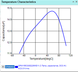
I am evaluating TPS62873EVM-144 (2phase of TPS62873) with Vin=3.3V, Vout=0.4V, Iout=24A and Cout=22uF(GRM155C80E226ME11) x4

I have a few questions:

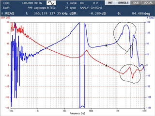
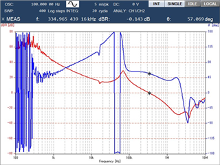
We are trying to optimize the phase compensation constants with an output capacitance of 22uF (GRM155C80E226ME11) x4, but we cannot find the optimal constants that satisfy both phase margin and gain margin. Specifically, even when reducing the gm amplifier output R1, the gain does not decrease, the fo remains high, and the phase margin does not change.
Is it impossible to optimize the G-Φ characteristics with phase compensation constants under this output capacitance condition?
Does the DCS control method require a certain minimum output capacitance to operate correctly?
Can we consider the formula shown in section 10.2.2.4 “Selecting the Output Capacitors” of the datasheet as the condition for the DCS control method to function?
In the Webench simulation, when setting the TPS62873 to 1-phase with an output capacitance of 22uF x4, Vout=0.4V, and Fsw=3MHz, the simulation does not work. Are there any constraints?

  • Hi,

    That is probably too little Cout.  Is there more located at your load?  The effective capacitance will also be lower than 22uF, due to the small case size.

    Page 5 of the D/S recommends a minimum of 40uF effective capacitance.  And this is per device.  Can you try with 3 or 4 of those caps on the output of each device?

    You can also try putting 2 of the output caps on each side of the inductor, near the IC.  Then, put the remaining 2 or 4 where C32 is, out by the load.

    What inductor are you using?

    Thanks,

    Chris

  • Hello, Chris


    I'm using XGL3512-900ME(Coilcraft) as output inductor.

    The effective capacitance GRM155C80E226ME11x4 at 0.4V is about 80uF.
    I trhink it satisfy 40uF effective capacitance per device. But I couldn't find the optimal constants of phase compensation.

    I want to know how to calculate or simulate minimum output capacitance to satisfy the G-Φ characteristics.
    Is the only way to find out through trial and error?

    Regards,

  • Let me ask you an additional question.

    Is it correct to understand that if the output capacity is insufficient, the G-Φ characteristic cannot be satisfied even if the phase compensation constant is adjusted, which is a phenomenon peculiar to DCS control? I want to know is the mechanism of insufficient of  outpuit capacitance and G-Φ characteristic  in DCS control.

    Regards,

  • Hi,

    Yes, you need more Cout.  Using SimSurfing, those caps only give 13-15uF effective Cout:

    There is a component calculator here for the module version, but it can also be used for this IC as well.  https://www.ti.com/tool/download/TPSM8287A-COMPONENT-CALCULATOR

    You need a certain minimum LC pole to keep the loop stable.  With the external compensation, you can adjust the loop gain but you can only reduce it to a certain point.  A lower LC corner frequency (from a higher L or higher Cout) helps keep the loop gain low enough.

    This app note describes this fixed-frequency DCS-Control topology in more detail: https://www.ti.com/lit/an/slyt846/slyt846.pdf

    If you can share your schematic, test results, and a photo of your board and test setup, I can help you debug.

    Thanks,

    Chris

  • Thanks, Chris.

    Since we are wasting time exchanging detailed information, I will first utilize the calculation tool you provided and proceed with the debugging.
    I have a question about how to use this tool.
    If the output current is constant at 20A, what is the input for ΔIout? Where should I enter the constant current?
    Also, how can I use this tool to estimate the phase margin?

    Regards,

  • Hello,

    I have measured the G-Φ characteristics using TPS62873EVM-144 (2phase of TPS62873).
    The +0.4V gain curve is changing to increase around 1.2MHz,
    The phase curve is significantly advanced between 1MHz and 2MHz.
    It would be helpful if you could comment on whether this characteristic is OK or not.

    Vin=3.3V
    Vout=+0.4V, +0.6V
    Iout=24A
    fsw=3MHz
    Cout=22uF(GRM155C80E226ME11) x12
    Lout=XGL3512-900ME(Coilcraft)
    Comp: R1=150Ω, C1=6.8nF, C2=10pF

    0.4V

    0.6V

  • Thank you for sharing.  Those bode plots look much better.

    The calculator does not calculate phase margin.  It uses the D/S equations, which are designed to give a stable design.

    Yes, the calculator is primarily setup for meeting a given load step.  If you have a constant current load, then you can skip those inputs and just focus on the Rcomp and Cout cells.  With a chosen Rcomp (which is usually very low, as you chose) make sure your Cout is greater than the required Cout.

    In your 0.4V plot, I would not worry about this.  It is at a very high frequency, and above the nyquist limit of bode plots which is fsw/2.  

    You might retest the 0.4Vout circuit with a 1.5 MHz fsw.  You are probably reaching the minimum on time at 3 MHz.  This is ok for the device, but may make the bode plot not look nice.

    Chris

  • Hello,


    This time, we have found a suitable output capacitance and phase compensation constant through trial and error. However, we don't want to repeat this trial-and-error process multiple times.


    This is a repeat of the same question, but could you please introduce any tools or formulas for determining the capacitance required to satisfy the phase margin?


    The tools you provided are useful for determining the voltage variation and output capacitance for step output in DCS control, but they do not provide information about the phase margin.


    I would like to know the mechanism, calculation method, and why 22uF (GRM155C80E226ME11) x12 is required to ensure phase margin in DCS control.


    (Webench simulation does not support 2-phase simulation for TPS62873. While 1-phase simulation is possible, it does not work under the conditions of Vout=0.4V and Fsw=3MHz. A Simplis model is available, but setting up the Simplis environment is costly, so it is not feasible for us)

  • Hi,

    The 3.3Vin to 0.4Vout at 3MHz design violates the minimum on time of the device, so Webench may not create a design for it.  Why do you want to operate at such high a frequency?  It is less efficient.

    The calculator can assist giving starting values for the loop compensation to satisfy stability.  You still need to measure your circuit with your components and validate that it is sufficiently stable.  To use the spreadsheet in this manner, enter your design inputs in cells C2, C3, C4, C12, and C14.  Set cell C18 equal to cell C16 or leave it at 300 kHz for a more conservative design.  Then, enter your actual effective capacitance used in cell C26.  Now, reduce Rcomp (cell C22) enough such that cell C25 is less than C26.

    Increasing Rcomp increases the control loop gain, while adding more Cout (or a higher L) decreases it.  The output filter needs to be strong enough to decrease the total gain enough to be stable.

    Chris