


Tool/software:
Hi,
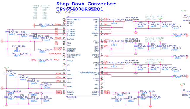
Please help to review schematic, thanks
Vin 12V,
Vout1 1.8V 0.5A,
Vout2 1.1V 3A,
Vout3 3.3V 0.1A,
Vout4 disable
Tool/software:
Hi,
Please help to review schematic, thanks
Vin 12V,
Vout1 1.8V 0.5A,
Vout2 1.1V 3A,
Vout3 3.3V 0.1A,
Vout4 disable

