This thread has been locked.

If you have a related question, please click the "Ask a related question" button in the top right corner. The newly created question will be automatically linked to this question.

TPS543C20A: PSPICE Trans Simulations

Part Number: TPS543C20A

Tool/software:

Hello,

I am using TI PSPICE to simulate the transients in my design.

I have been able to successfully run the simulations as is from the TI TPS543C20A downloads page. 

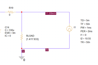
I also was able to alter the startup trans simulation to step to 14v and output at 1.4v @28.3A using my circuit set up.

I'm currently trying to alter the simulation in order to see the effects of stepping the load current from 17.833A to 29A.

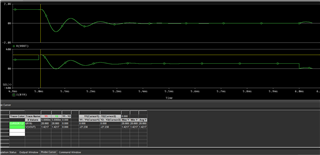
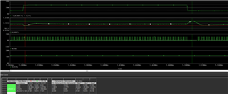
I've not had any success with this. The most common issue I have is there is never a convergence. 

The simulation I am interested in is a 50nS load current increase from 17.833A to 29A once the switcher is already outputting 17.833A at 1.4v with a steady 14v in. 

I am inexperienced with PSPICE and could use some help, I've hit a bit of a wall trying to get this to work.

Thanks,

Matt

  • Hi Matt, 

    I will certainly take a look into this. To save some time, are you able to attach your design that is running successfully with constant load current. That way I can alter the load without reselecting components to match your design. This also will help me recognize where something might be off in your current file, if it exists

    Best regards,

    Britton

  • Hi Britton,

    Attached is the simulation file that shows what I am trying to do. So, I've swapped the input voltage source with a 14v dc source. Then set the feedback resistors to give a 1.43V output voltage.

    I am trying to get the simulation to steady state 1.43v output at ~17.8A then step the load current by 10.55A to ~28.33A.

    The current jump should be 50nS to accurately model our system. 

    I've attempted placing a current source in parallel with the load resistance and setting it on a delay until a steady state set voltage/current is reached, then pulsing it with 50nS rise time from 0 to 10.55A. This doesn't seem to work.  The output voltage/current drops to nothing basically when the current source switches on. I'm trying to use the current source like a sink.

    I think from you will have a pretty good Idea of what I am trying to accomplish.

    Thank you,

    Matt


    TPS543C20A_PSPICE_TRANS.zip

  • Thanks Matt. I'll take a look at this as soon as possible and get back to you tomorrow or the next day

    Best regards,

    Britton

  • Hi Britton,

    Were you able to make any progress on assisting me with the simulation?

    Thanks,

    Matt

  • Hi Matt, 

    I was able to take a look at this. I recommend to capture all steady state data at 17.8 in a separate simulation and then simulate the load transient step independently. To simulate the load transient step from 10A to 28A, you can do the below:
    1. Set a load resistor with the minimum current (10A). I recommend a resistor with the value set to {1.4/10}

    2. Set a pulse current source in parallel with the load resistor with the I1 set to 0 and I2 set to 18A. Ensure the time delay is longer than it takes the device to reach steady state at the minimum load current (10A).

    It is likely to run into issues when trying to maintain 17A, then step down to 10A, then back up to 28A in a single simulation. You might try to simulate a load transient step from the steady state 17A to the minimum load current (10A) separately from the 10A - 28A step if the data is applicable for your case.

    Best regards,

    Britton

  • Hi Britton,

    So, for 2. I've tried this. I retried it. Below is the configuration at the load:


    Here are the results from the simulation. The top Plot is vout and the bottom is the current from R19( I used this series resistor in order to get a plot of the full load current instead of a piecewise one. )

    You can see initially the current jumps and the voltage holds then shortly after the load current and output voltage drop.

    I'm not sure what to interpret here. 

    1. Is this the actual response and if I let the simulation run longer it is slowly going to respond milliseconds later?

        I'd have thought the response would be a little closer to accomplishing the output in this time window. Note I originally ran this setup as you suggested before I sent you the simulation the first time and let it run longer and I never saw the output recover, I think this was a 15mS window vs the current 6mS.

    2. Is my setup incorrect?  Note I have 187K resistor on my ramp pin. In the actual design I am not using this pin at all.

    Specifically, I am asking can you explain what I am seeing when the current source turns on.

    Should I expect this response from the switcher, or am I configuring something in the circuit incorrectly?

    Thanks,

    Matt

  • Hi Matt, 

    That's strange. From the screenshot attached it looks like your configuration is correct. This is not the expected response of the converter and it should be able to simulate this step. I will match your schematic and share my project with you by Monday. My hunch is that something small is up with the schematic.

    By the way, you can reduce the SS time and initial rise time of the VIN source to bring up the device quicker if the 5ms simulations are taking too long.

    Best regards,

    Britton

  • Hi Britton,

    Have you been able to pinpoint the error in the schematic yet?

    Thanks,

    Matt

  • Hi Matt, 

    I did get the chance to look into this today and I'll share my findings below.

    It seems that the convergence errors were persistent, unless I ensured the following:

    1. Remove the 0ohm R19 resistor. In order to measure the combined current of RLOAD and I1, you can do trace math by right clicking on the plot, Add Trace, then filling in the trace expression box with I(RLOAD)+I(I1). 

    2. Go to simulation settings and ensure that Skip initial transient bias point calculation (SKIPBP) is selected

    3. Use a nearby voltage setting to 1.4V. I was unable to converge the simulation when the feedback resistor divider was connected to the VOUT node. However, when VOUT is tied directly to RSP, the simulation converged successfully. This is unintended, but to validate your transient condition, you can use all of the same BOM, except use the 1.1V VOUT setting by setting VSEL to 187k. The overshoot and undershoot performance will be comparable to 1.4VOUT. 

    Alternatively, you may use the excel calculator tool to estimate the load transient performance at 1.4VOUT by filling in your load step size, rate, and viewing the resulting Overshoot and Undershoot calculations. 

    Here are my results and schematic from doing a 1.1V load step using the adjustments listed above.

    Best regards,

    Britton