This thread has been locked.

If you have a related question, please click the "Ask a related question" button in the top right corner. The newly created question will be automatically linked to this question.

Noise coupling with GNSS receiver

Part Number: BQ24253

Tool/software:

Hello,

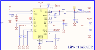
I am using the BQ24253 charger to charge a 1 cell lipo battery.

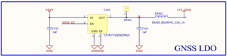
The input of the charger is 5V from a DC-DC converter. The output of the charger, VSYS voltage is used to supply a GNSS receiver througn a LDO.

Below the schematic of the charger and the LDO.

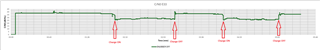
When I enable the charger, the C/N0 of the GNSS receiver is attenuated with almost 10dB.

Below the graph of the C/N0 for one sattelite.

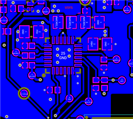
Below the layout of the charger :

  • Hello, 

    Please see below for suggested techniques to reduce noise due to switching converter of BQ24253 IC. 

    1) Add a 1 nF capacitor at PMID, SYS, IN (optional), and BAT (optional). The purpose is to add this high frequency cap which works in 100MHz to 200MHz range to return high frequency noise to GND. 

    2)Add resistor (in range of 0 ohm to 10 ohm) in series with BOOT capacitor from BOOT pin to SW pin. The purpose is to reduce the switching slew rate. We do not recommend using higher resistors values than 10 ohm as it will start to adversely affect converter efficiency.

    3)Add a snubber circuit (resistor and capacitor) from SW pin to GND. Use R = 1ohm and C = 15 nF as reference, but TI recommends to try several different combinations to get best results with your custom PCB design. 

    I have also reviewed the provided layout and do not see any obvious concerns. The layout for your design follows the layout guidelines listed in datasheet section 12.1. 

    Best Regards,

    Garrett