Because of the holidays, TI E2E™ design support forum responses will be delayed from Dec. 25 through Jan. 2. Thank you for your patience.

This thread has been locked.

If you have a related question, please click the "Ask a related question" button in the top right corner. The newly created question will be automatically linked to this question.

TPS92682-Q1: MOSFET damage during supply power rising slowly

Part Number: TPS92682-Q1

Tool/software:

Hi Team,

We found the MOSFET of TPS92682 can be damaged when we are testing the supply voltage slowly rising condition.

The slow voltage rising is from 0V to 20V, duration is 45s. When the supply voltage reached 6V, the TPS92682 started output(enabled), then it enters limp home mode. According to our configuration, limp home mode is 1A output current.

According to this waveform, it indeed entered the limp home mode, but output current and input current both rising slowly. And the output current reached 1.6A, input current increased to 20A as well. Then the MOSFET damaged.

We tested the Gate duty cycle at the waveform condition, the duty cycle is 92%, which is already the max duty cycle. And we suspect the MOSFET damage is due to high duty cycle.

Yellow=input voltage, green=input current, pink=output current. 
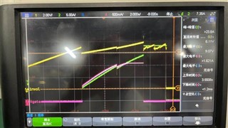
We try to do some analysis on the efficiency, 

Here is another waveform:

Yellow=output voltage, blue=input voltage, green=input current, pink=output current
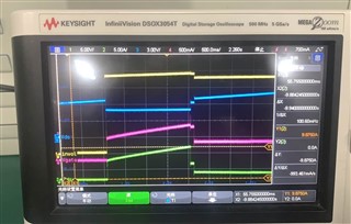
Based on this, we found the efficiency is around 56%, seems too low.

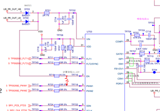
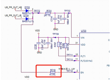
Here is the schematic if needed

07.pdf

Our questions are:

1. Why cannot the output current get to target 1A after the enable? Why there is a slowly rising on this current waveform?

2. Why it continues increase to 1.6A in limp home mode? Is it because loop control doesn't close?

3. When the input voltage is 6V, we tested the VCC voltage, it is 4.5V. Would this be an abnormal status?

Thanks

Best,

Frank

  • Hello Frank,

    Can you give us the design requirements.  Operating range?  Vin(min, typ, max)?  Output current (min, typ, max)?  It looks like a CC Sepic, please confirm.  We will also want all the register setting.  I think we need to see the inductor current going into the main switch fet, the switch node (Drain of FET), Vin, and Vout.  We may also need close ups/zooms of waveforms.  Make sure the scope waveforms are properly labeled.  Also, can we get actual waveform images from the scope instead of phone pictures?  

    At low line the input currents can be huge which will mean large losses due to Rds*I^2.  Are they getting faults during the startup?  Why is the input voltage dropping so much as the supply ramps up?  I don't understand that? Are you sure you aren't hitting UVLO and resetting the part?  Do we have a diagram of their test setup?  I also don't know when in this time period the SPI commands are coming in to program the part or to reprogram the part during this condition?  Did you look at the gate of the switching fet?  Can I see waveforms for this?  I am concern the voltage is lower than it should be and it could cause the switching fet to have higher resistance than normal, which could cause excessive power losses.  Also, if you have that high an input current why isn't it triggering current limit?  We may need to adjust that.  Can you tell me the part number of the inductor?  I want to make sure we aren't saturating it at low line.  I want to see the datasheet.  

    This might take some time to figure out why this is failing.  Is getting a board shipped to us to look at waveforms and option?  Please let us know.  

    -fhoude

  • Hi Francis,

    Please check our responds below:

    It is SEPIC CC mode. We will try to get the register configuration later.

    The slow power up test is configured as powered from 0V to 20V, ramp up takes 45s. When supply voltage is 6V, TPS92682 just started work, the limp home mode was triggered. At this mode, the output current is set as 1A.

    The normal operation is 9-16Vin, output is 1A. When voltage between 6.5V~9V and 16V~19V, it is linear power decreased. it is output 400mA at 6.5V, 1A at 9V.

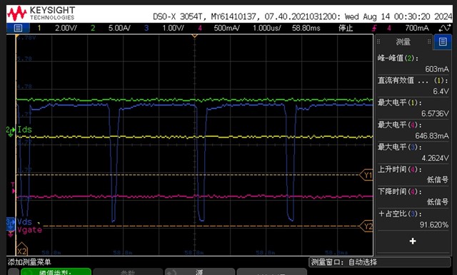
    The waveform of Gate(blue) waveform at 6V is attached below. The duty cycle is 91.62%, Gate max voltage is 4.26V.

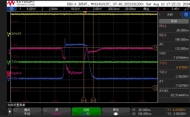
    When it is low voltage condition, the Gate(pink) and Drain(blue) waveform:

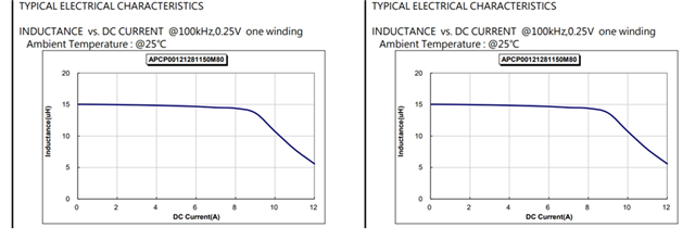
    The inductor P/N is APCP00121281150M80, the datasheet please refer this link:

    APCP_Series.xls (chilisin.com)

    We agree it is complex, so we are working on more investigation now. We would like to get your insight on:

    • Why is the voltage rising so slow after enable? Is this a correct operation? And we don't understand why it keep rising after reached 1V configured output voltage.
    • What is the working status between 4.5V~6V, can it operate the same as over 6.5V? We suspect the device is not in correct operation.
    • Does the MOSFET didn't fully turn on? MOSFET is  BUK7Y14-80E (N-channel 80 V, 14 mΩ standard level MOSFET in LFPAK56) | Nexperia
    • For SEPIC CC mode, when Vin is low voltage, typically it will show low efficiency?

    Thanks for your support

    Best,

    Frank

  • Hi Team,

    Looking forward the ideas. Thanks

    Best,

    Frank

  • What is the load?  If LED, then number of LEDs and the Vf of the LED at that min and max loads.  Vf vs If curve would be good.  

    Do you have any circuitry for UVLO, such that it doesn't try to operate until it reaches 9Vin?  You could use the EN pin and add a resistor to the 1k pull up.  The EN threshold is 1.21V with 100mV hysteresis.  

  • Hi,

    Right now we are using a 1k pull up at EN pin. Do you want to add another 1k?

    The LED number is 8, 3W for each LED. Vf is between 24-27V.

    There is no other circuit for UVLO. Do you have recommendation for UVLO circuitry?

    Thanks

    Best,

    Frank

  • Frank, 

    Besides 1k resistor pullup resistor, you need to add a resister from EN pin to Gnd as voltage divider for UVLO setting. 

  • Hi Xiaoguang,

    Thanks for the reply on UVLO.

    While the initial question is still open, we would like to know why is the voltage rising so slow after enable? Is this a correct operation? And we don't understand why it keep rising after reached 1V configured output voltage.

    Thanks

    Best,

    Frank

  • Frank, 

    Actually, I'm unable to understand the tested waveforms. Why Vds keeps on/off while Vgate is in 500mA/div?  

    For below waveform, what is invol? it looks like 9V. Is it input voltage? Why Ids = 0 ? 

    You need to share correct tested waveform that can explain what happens.