This thread has been locked.

If you have a related question, please click the "Ask a related question" button in the top right corner. The newly created question will be automatically linked to this question.

TPS23753A: design review request

Part Number: TPS23753A

Tool/software:

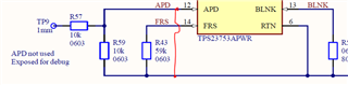
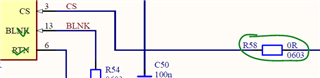
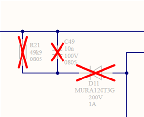
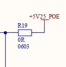
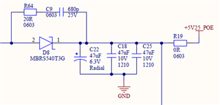
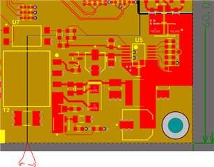
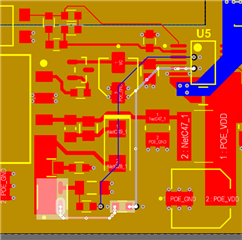
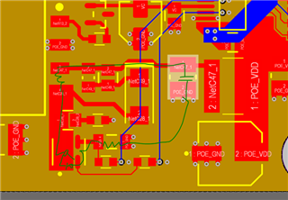
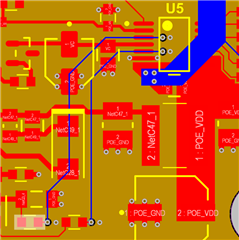
I just finished implementation of the TPS23753A, mostly based on the schematic of the TPS23753AEVM-001

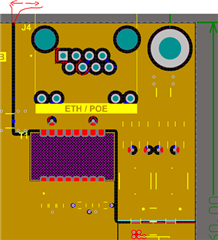
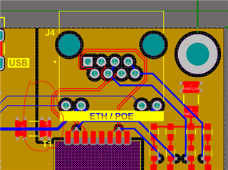
My stack-up is four layers and single sided assembly, so it differs a bit from the EVM lay-out.

Is it possible to get a review of the schematic and layout? That would help me out a lot and might prevent unneeded errors.

The files are confidential, so I prefer to send them by mail.

Thanks in advance,
Jesse

  • Hi Jesse,

    Thanks for reaching out!

    Yes we can help to review the PoE schematic (pdf.) and layout (.brd). I will reach out in email.

    Best regards,

    Diang 

  • Just replied to your mail, thanks!

  • Hi Jesse,

    Thanks and confirmed received the file. I will start from the schematic and get back to you in 3 business days. For the layout, is it possible to send a brd. version file or PCB original file? Thanks!

    Best regards,

    Diang

  • Hi Jesse,

    Please see the comments on schematic below. For the layout, is it possible to send a brd. version file or PCB original file? Thanks!

    1. You can tie APD to RTN if not using adapter. It is also ok to keep the current circuit.


    2. It is recommended to add a 1k resistor and a cap between CS and RTN with 47 – 100 pF in case there is any noise.


    3. It is recommended to populate the passive RCD clamping circuit to release the leakage inductance energy and reduce the switching overshoot.

    4. POE70P-50L is rated for 7W. Please check if the output exceeds 1.4A?


    5. The output capacitance could be further increased. Higher capacitance is recommended for low output voltage. Ceramic cap may have capacitance reduce at high voltage.

    Best regards,

    Diang

  • Thanks for the schematic feedback.

    Point 3) It's DNP in the EVM, but I can populate it just in case.

    4) This was copied from the EVM. Would you recommend adding an extra electrolytic, or adding MLCC?

    I am looking forward to the feedback on the layout. 
    ODB/Gerber should easily be viewable using online viewers, but I can send you the original Altium file if that helps.

  • Hi Jesse,

    Yes, it would be very helpful to share the Altium in email. Thanks!

     For 4), it depends on the power output. If your output is below 5V/1.4A, it should be fine.

    Best regards,

    Diang

  • Hi Jesse,

    Please see the layout review comments below. I also attached a layout review check list which may help. Let me know if you have further questions. 0250.PoE PD Layout Check LIst.xlsx

    1. The isolation between chassis and data ground is better to be higher than 1.5kV rms. Besides, some blue wires crosses the isolation polygons, which eliminates the isolation.

    2. The isolation between PoE input and output ground is better to be higher than 1.5kV rms.

    3. The gate loop is too long and the gate path width is too thin (> 20 mils width is recommended).

    4. The power loop is too long. And the power path is too thin (> 50 mils width or polygon is recommended).


    5. The current sense RC needs to be close to the PWM chip (TPS23753A)

    Best regards,

    Diang

  • Thanks Diang, I will apply the suggestions and continue with production.

  • Hi Jesse,

    You are welcome! I will close this thread for now. Please feel free to let me know if you have further questions or concerns. 

    Best regards,

    Diang