Other Parts Discussed in Thread: BQ40Z50, EV2400
Tool/software:
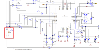
I’m designing my first 4-layer PCB for a 2-cell battery monitoring system using the BQ40Z50 BMS chip.

According to the datasheet and reference design, it’s recommended to create two separate grounds: one for the fuel gauge and one for the charger. I’ve implemented this separation, but I’m having trouble deciding how to attach them together properly.
Additionally, the power lines on this board need to handle currents ranging from 10A to 15A. Here’s a summary of my design and questions:
Current Stackup: Top Layer: Signal/Power Inner Layer 1: GND Plane Inner Layer 2: GND Plane Bottom Layer: Signal/Power Key Concerns: Ground Separation: How should I connect the separate grounds for the fuel gauge and charger to ensure proper functionality without introducing noise or other issues?
Power Trace Width: I need to confirm that my power trace width is sufficient for handling 10-15A. Should I consider increasing the copper thickness to 3 oz or 4 oz, or would it be better to implement double power lanes (one over another)? Any tools or calculators for determining the correct trace width would be greatly appreciated.
Thermal Management: Should I be using vias for better thermal management, or are there other recommendations for ensuring the board stays cool under high current? Are there any stackup adjustments or other considerations I might have missed?
Since this is my first 4-layer design, I’m sure there might be things I’m overlooking. Any advice or feedback on these issues would be very helpful. This my board.
Thank you in advance for your guidance!