This thread has been locked.

If you have a related question, please click the "Ask a related question" button in the top right corner. The newly created question will be automatically linked to this question.

UCC28951-Q1: Resonant ring

Part Number: UCC28951-Q1
Other Parts Discussed in Thread: UCC28951

Tool/software:

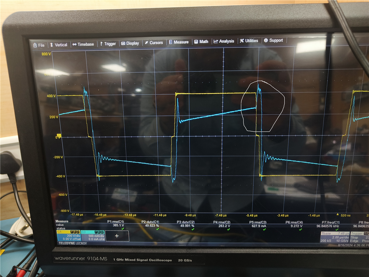
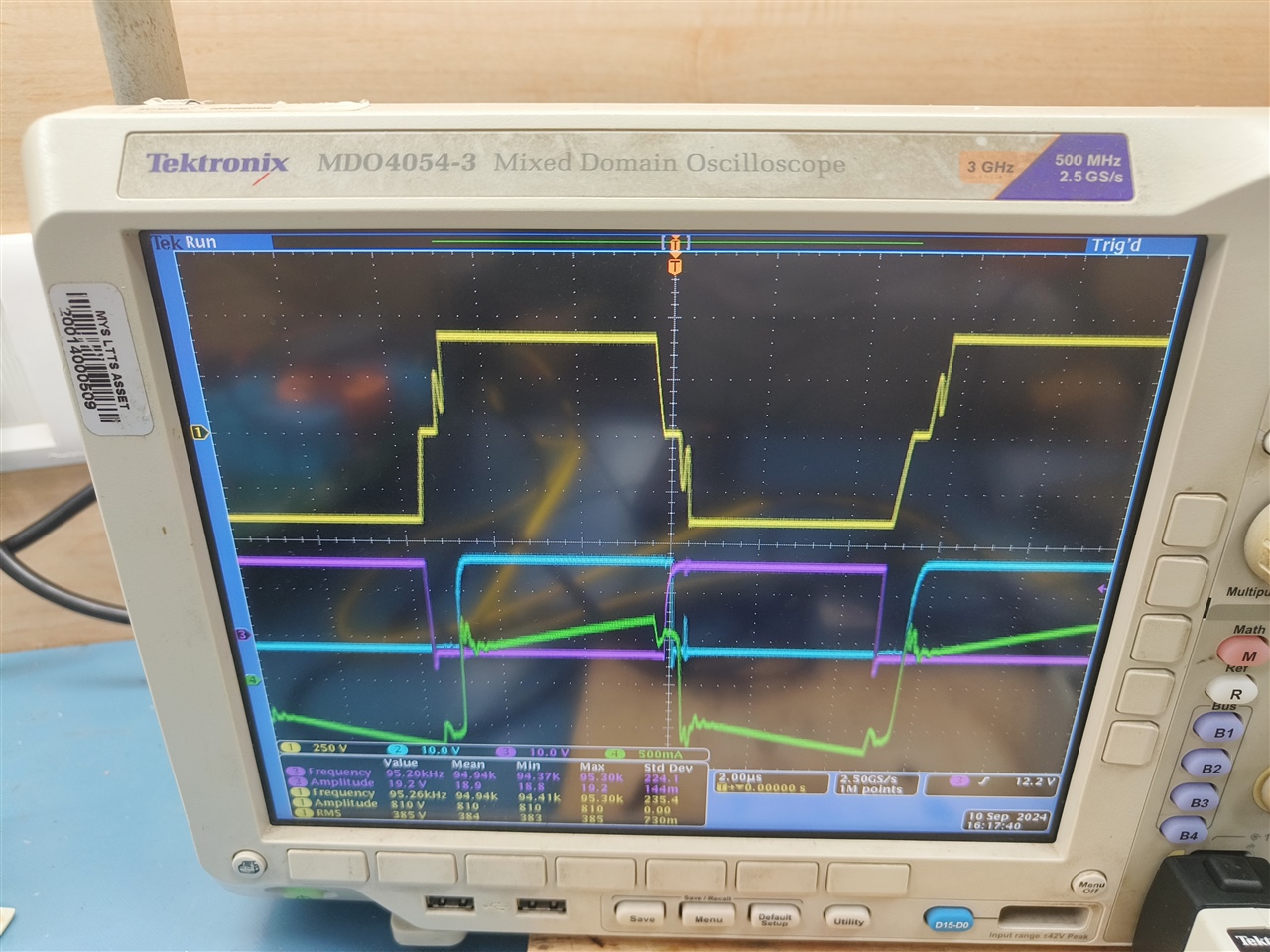
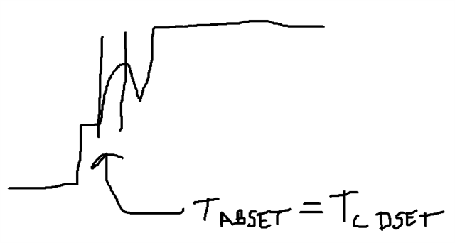
The voltage ring at transformer primary voltage is disappeared with reducing fixed delays.

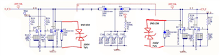
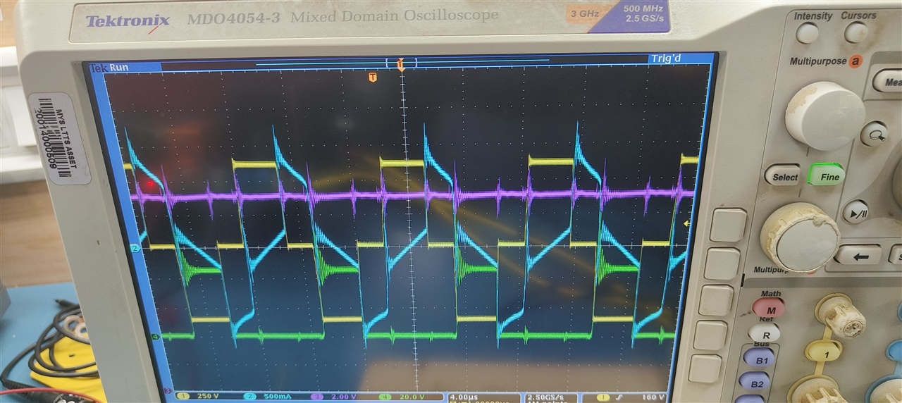
FYI, TURNS RATIO : 27, Lmag: 8mH primary , Llkg :22uH

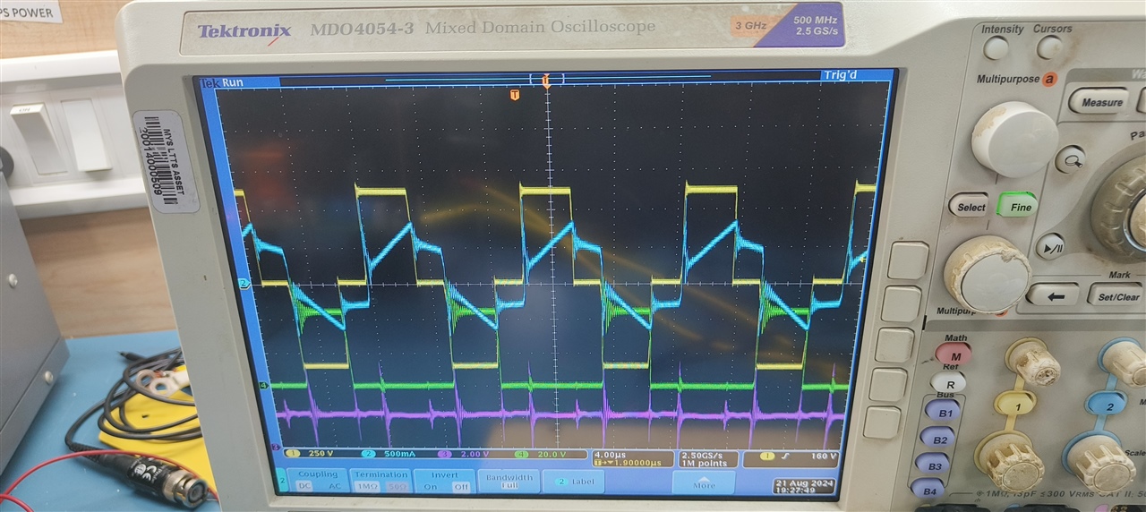
1. Vin : 600V, higher load currents , 20A and above

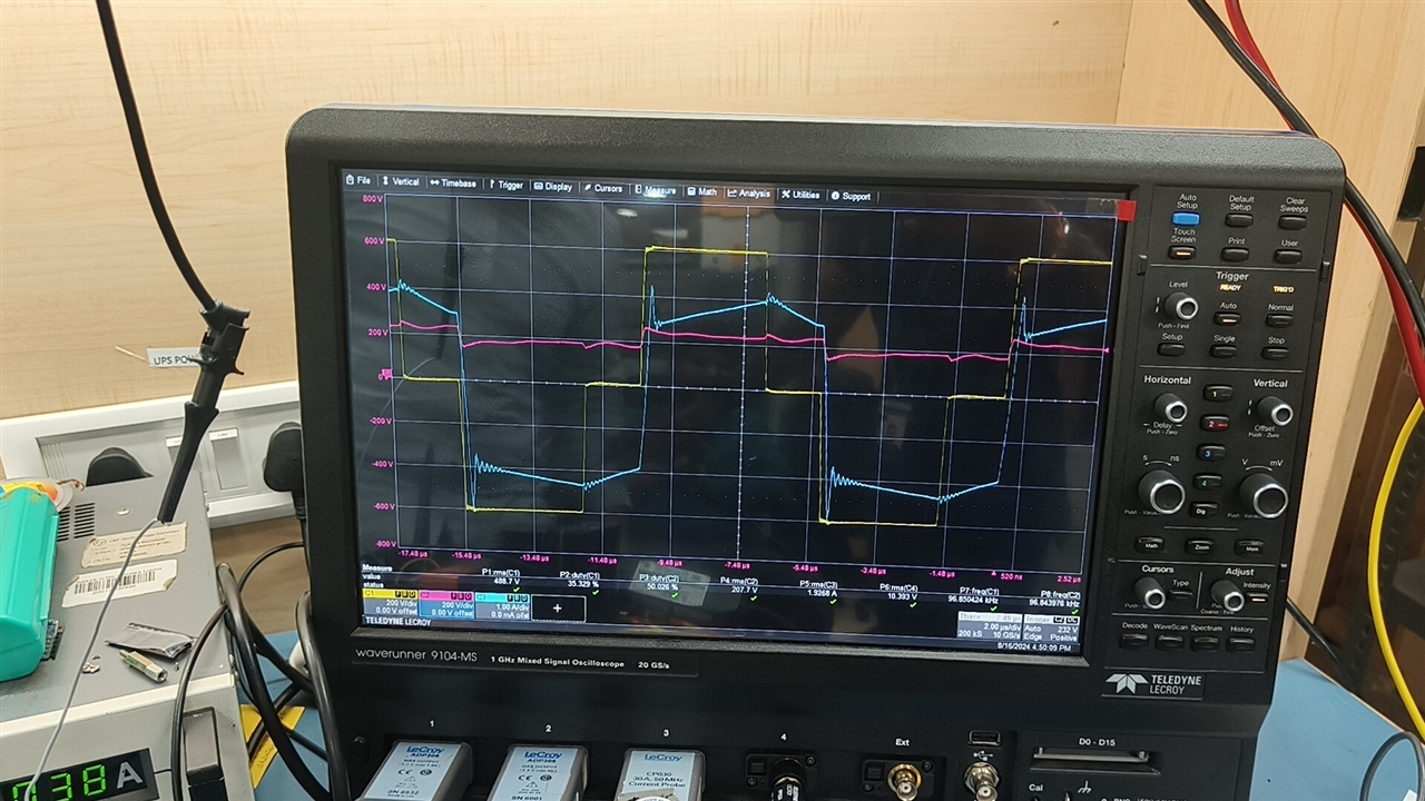
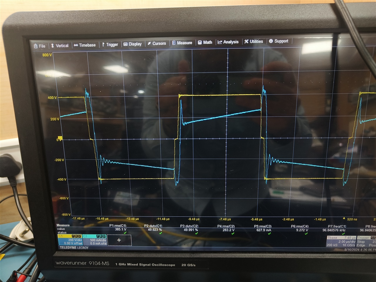
Yellow: primary transformer voltage 

Blue : transformer primary current 

2. At lower voltages , for example at Vin :400V, 450V,  load current:15A,

the current waveform at freewheeling period is increasing in other direction. Is it alright? Any reason why ? Is it due to low load current or high turns ratio ( 27 ) or anything else ??

  • Hello,

    Your inquiry has been received and is under review.

    Regards,

  • Hi.

    This is Normal case only

    During first one conduction via Mosfet for certain time Ramp up current,&n via Diodes at downslope time

    second case Phase shift is maximum and very short span allowing diodes to freewheel that why it seems 

    Reason for this is Winding capacitance, stray capacitance of switches, diodes and leakage inductance

    Anyhow its good to proceed with your testing,maybe snubber at secondary side required if secondary voltages having voltage overshoots

    Thank you

    venkatesh B

  • 1. What should be ideal winding capacitance ? Should it b less or more, what steps to take if it's more ?

    2. When you say phase shift is maximum , please explain this more in simpler terms for better understanding. Sic antiparallel diodes are placed. And MOSFETs are also SIC. 

    MOSFET P/N: G3R160mt12d

    Diode p/n : gd02mps12e

    3. Ringing in the current waveform, how to reduce it ? Can we try some RC snubber across CT ? Or what is your suggestions.

    4. What values you suggest for SNUbber at secondary side . Please advise 

  • Hello,

    I am not sure what you are seeing is parasitic capacitance.  At the end of your free wheeling before the current changes polarity there is a flat spot in the current waveform.   This flat spot is roughly 400 ns. This should not be the case you should still see the inductor down slope.  So why don't you see the inductor down slope?

    When you go to max duty cycle during the free wheeling period which is equal to 400 ns.  The current spikes and the inductor down slop is not seen.  This behavior should not be there. 

    Are you doing something non traditional on the output of your design?  Could you share the schematic for review?

    Regards,

  • Hello Mike,

    1. The below is the schematic for both windings. Winding 1 and Winding 2, both have same components.

    Presently Secondary Mosfets I'm using is IRF200P223. Schottky diode is added for faster turn OFF. 200V TVS is added for snubbing. 

    Winding 1 and winding 2 presently are connected in parallel combination, not in series.

    At primary side, 4 SiC MOsfets , Anti parallel diodes, Transformer with Llkg:22uH is connected.

    Primary MOSFET P/N: G3R160mt12d

    Diode p/n : gd02mps12e

    FYI, With increasing Higher voltages, higher load currents, That rise in current waveform totally diminishes and there is a downslope as usual during the freewheeling period.

    2. Ringing in the current waveform, how to reduce it ? Can we try some RC snubber across CT? Or what is your suggestions.

  • Hello,

    When your design goes into freewheeling from this maximum duty cycle the transformer current should decrease with inductor current.  In you waveform it jumps up with a greater magnitude then it went into free wheeling.  This should not happen.   It is almost as if one of your SRs is shorting out the output inductor.

    You might want to double check how your output transformer windings are connected to the output filter.

    Regards,

  • Hello Mike,

    1. What I noticed about that jump in current is, when I run secondary FETs in diode mode, that Jump is not present. When I turn the FETs ON, only at that time that jump is present.


    When gate signals are OFF 

    Blue: primary current 

    When gate signals are ON

    2.Additionally, When current changes direction, The rise in current, we are seeing noise / ringing at gate signals of synchronous FETs. Your comments and advise

    3. Can Synchronous FETs overlap for some duration? As een in my case ?

    4. Another thing is ringing in primary current waveforms, how to reduce it?

    5. Secondary side FETs have ringing across drain to source during switching, though RCD clamp is present. How to mitigate??

  • Hello,

    Your inquiry has been received and is under review.

    Regards,

  • Hello,

    Please see my comments below.

    1. What I noticed about that jump in current is, when I run secondary FETs in diode mode, that Jump is not present. When I turn the FETs ON, only at that time that jump is present.


    When gate signals are OFF 

    > The transformer primary current does not look correct during the freewheeling cycle when the transformer current is negative.  It should look like the transformer current when the current is positive.  There might be something wrong in the way your output rectifiers are connected in your design.  You should double check this.

    Blue: primary current 

    When gate signals are ON

    >Not sure what the below waveform is.  Can you double check this?

    2.Additionally, When current changes direction, The rise in current, we are seeing noise / ringing at gate signals of synchronous FETs. Your comments and advise

    3. Can Synchronous FETs overlap for some duration? As een in my case ?

    >Yes during the freewheeling period both FETs are on.


    4. Another thing is ringing in primary current waveforms, how to reduce it?

    >Your transformer primary current waveforms do not look correct.  I believe that there is something not connected correctly in your power stage.  I would double check it against application note slua560.

    https://www.ti.com/lit/pdf/slua560

    5. Secondary side FETs have ringing across drain to source during switching, though RCD clamp is present. How to mitigate??

    > I would start by figuring out why the primary transformer current is not correct.  Once you have figured out what is causing that issue you can move on and try to fix the ringing if it is still present.

    Regards,

  • Hello Mike, below is transformer waveforms.

    1. Could you explain is this related to delays ? And what can be done to mitigate it ? Reduce delay??

    2. Additionally how to avoid leading edge current spike ? It increases with increase in voltage. 

  • Hello,

    Your inquiry is under review and I will get back to you shortly.

    Regards,

  • Hello,

    The spikes are actually the resonant ring between the switch node capacitance and your shim inductor (Ls), leakage inductance Llk and switch node capacitance (Csw).

    Your are correct that his to do with your delays TABSET and TCDSET.  They are are to long.  You need to set the delays to 1/4 the resonant frequency please note the equation is below for setting the initial delay.  

    TABSET = TCDSET = 1/(4*(*2*3.14*(Csw*(Ls+Llk)^0.5))

    I also drew a picture where this delay should be set. Your delay is just to long.

    The following link will bring you to an application note that goes through the step by step design process of using the UCC28951 in a phase shifted full bridge converter.  You might find this information helpful in your design process.

    https://www.ti.com/lit/pdf/slua560

    Thank you for interest in Texas Instruments (TI) products.  If you have a related question, please click the "Ask a related question" button in the top right corner. The newly created question will be automatically linked to this question.

    Regards,