This thread has been locked.

If you have a related question, please click the "Ask a related question" button in the top right corner. The newly created question will be automatically linked to this question.

TPS7B4255-Q1: EE test

Part Number: TPS7B4255-Q1
Other Parts Discussed in Thread: TPS7B4255

Tool/software:

Hi team,

My customer says they will do EE test to TPS7B4255-Q1 and wonders if TPS7B4255-Q1 can meet this test. (Customer says competitor's device cannot meet this test.) The following is the test method.

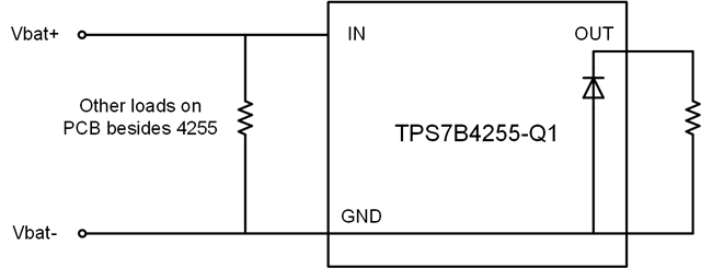
1) Disconnect DC supply's GND with PCB's GND.

2) Connect DC supply's GND with TPS7B4255-Q1's out pin and last for 60s.

There're 2 points customer is concerned about:

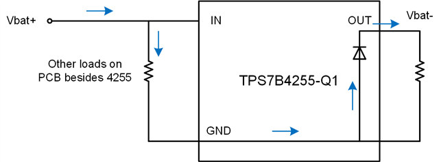
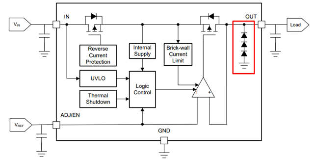
1) When DC supply's GND is disconnected (hot-swap), there will be a negative overshoot voltage at IN pin of 4255, which will be coupled to the OUT pin through input capacitor and output capacitor. And there will be a microsecond negative voltage at OUT pin (about -10V to GND). Will this negative voltage damage the device?

2) The positive and negative poles of the DC supply are connected to the IN and OUT pins of the 4255 and last for 60 seconds. Will this damage the device?

Thanks and looking forward to your reply.

BR,

Grey

  • Hi Grey,

    1. A voltage of -10V at OUT might damage the device. The abs min value for TPS7B4255's VOUT is -5V referenced to device GND. 

    2. What is the voltage setting for the DC supply? The device can withstand -40 to 40V maximum for VIN - VOUT. Any voltage difference beyond this value will damage the device.

    Thanks and Best regards

    Ishaan

  • Hi Ishaan,

    Thanks for reply.

    2. DC supply is voltage of battery, the range is within -40 to 40V. But there is another concern: when the DC supply is connected normally to the board, the circuit is like pic shown below. I made the other loads besides 4255 equivalent to a resistor.

    When the cathode of DC supply is disconnected from the GND and connected to the OUT pin, there is a current loop from Vbat+ to Vbat-, when means the diode of OUT pin will carry the current from other loads on the board. According to customer, the current is about hundreds of mA, less than 1A.

    Can the diode of TPS7B4255-Q1 carry such current and not be damaged? (last for 60s)

    Thanks!

    BR

    Grey

  • Hi Grey. I have asked our design team to confirm what current these diodes were sized for. I will update here as soon as I get a response.

  • Hi Ishaan,

    Thanks for following up. Is there any update from design team?

  • Hi Grey

    I haven't yet heard back with a definite answer. They are running some simulations. I will update here once they get back to me.

  • This is what I got from the design team 

    "Knowing the requirement, I would say we can’t support >100uA current when VOUT is clamped to negative.

    It was not asked from definition to support current, however because of the -ve clamp that was designed based out of Zener, current path from ground is limited by the resistor depending on the VOUT(-ve) value.

    Other path from GGNMOS cant support DC current as this cell is meant for the ESD path."