


Tool/software:
hi,
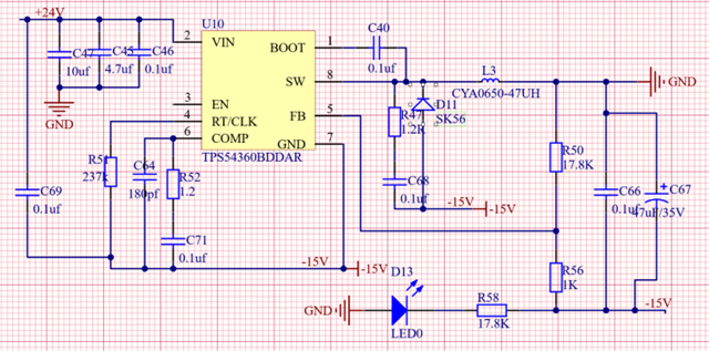
The customer is using TPS54360B for an output voltage of -15V, an output current of around 0.5A, and an input voltage of 24V. Please help review the schematic diagram. Thank you!
Tool/software:
hi,
The customer is using TPS54360B for an output voltage of -15V, an output current of around 0.5A, and an input voltage of 24V. Please help review the schematic diagram. Thank you!

