This thread has been locked.

If you have a related question, please click the "Ask a related question" button in the top right corner. The newly created question will be automatically linked to this question.

LM61480: Is there any problem with a GND pattern under the inductance(L1)?

Part Number: LM61480

Tool/software:

Dear Specialists,

My customer is considering LM61480 and has a question.

I would be grateful if you could advise.

---

I am currently designing a peripheral circuit for the LM61480.
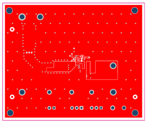
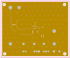
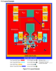
According to the LM61480 data sheet P.50 11.2 Layout Example has a GND pattern directly under L1.
It is generally considered better to remove the GND directly under it.
Is it correct to say that the LM61480 recommends that the pattern directly under the inductance be filled with GND?

Is there any problem with a GND pattern directly under the inductance?

---

I appreciate your great help in advance.

Best regards,

Shinichi

  • Hi Shinichi,

    The datasheet shows the recommended layout and is similar to the layout present on the EVM. 

    From my understanding, the consideration to remove the GND below the inductor applies more to older unshielded inductors where the coupling of SW with the GND plane can affect EMI performance by forming an antenna. Some engineers seem to favor this method for older devices.

    However, with this device, TI recommends the layout above with the GND plane intact underneath the inductor. This provides better thermal dissipation and can help block common-mode noise, which is critical for this design. Additionally, with a shielded inductor, the eddy current leakage is small and the potential EMI drawback behind an intact GND plane beneath the inductor is minimal. Please also ensure that layer 2 of the PCB is a GND plane as this acts as the device's main noise shield.

    Thank you,

    Joshua Austria

  • Hi Joshua,

    Thank you for your reply.

    I understand if a shielded inductor is used in the circuit, it's not a problem.

    Where can I find the EVM documentation you mentioned?

    I'd like to share the layout example with the customer.

    However, I cannot find in the product folder.

    Could you please let me know?

    I appreciate your great help and cooperation.

    Best regards,

    Shinichi

  • Hi Shinichi,

    When I said "layout above" I meant the layout picture you shared from the datasheet. Apologies for any confusion.

    Thank you,

    Joshua Austria

  • Hi Joshua,

    Thank you for your reply.

    I understand there is not EVM at this time.

    And let me confirm.

    Does that mean that the layer just below the inductance is GND?

    Please also ensure that layer 2 of the PCB is a GND plane as this acts as the device's main noise shield.

    I appreciate your great help and cooperation.

    Best regards,

    Shinichi

  • Hi Shinichi,

    Yes, the 2nd layer of the PCB should be a GND plane. This is a different EVM but here is an example:

    Layer 1: Top Side

    Layer 2: GND

    Thank you,

    Joshua Austria

  • Hi Joshua,

    Thank you for your reply.

    I understand.

    I'll share this information with the customer. 

    Also, the customer has additional questions.

    Could you please advise?

    ---

    ① Even taking into account the capacitance between the terminals, would it be better to have a GND pattern under the inductance?

    ② You mentioned that placing a GND below the inductor helps block common mode noise.

    Could you please explain this in more detail?

    ---

    I appreciate your great help and cooperation.

    Best regards,

    Shinichi

  • Hi Shinichi,

    Yes, the GND underneath the inductor, would provide more thermal dissipation for the device.

    About the common mode noise, a ground plane provides a shield from the switch noise that emanates from the SW node. As current switches through the inductor, it generates a magnetic field. This essentially creates switching noise. If there is a cutout beneath the inductor, the magnetic field from the inductor can freely enter the other layers and potentially introduce noise in the rest of the system. This is why we also recommend routing sensitive traces away from noise sources such as the SW node. By pouring GND below the inductor, you GND the magnetic fields and reduce the amount of noise that would enter the rest of the PCB. 

    Thank you,

    Joshua Austria

  • Hi Joshua,

    Thank you for your quick reply.

    By pouring GND below the inductor, you GND the magnetic fields and reduce the amount of noise that would enter the rest of the PCB. 

    You mean, by placing a ground pattern under the inductor, the magnetic field is shielded with ground, reducing the amount of noise that gets into the rest of the PCB.

    I appreciate your great help and cooperation.

    Best regards,

    Shinichi 

  • Hi Shinichi,

    Yes. This is why the GND pour underneath the inductor is recommended and a full GND layer underneath the top side to ensure that any signal traces underneath are sufficiently shielded.

    Thank you,

    Joshua Austria