This thread has been locked.

If you have a related question, please click the "Ask a related question" button in the top right corner. The newly created question will be automatically linked to this question.

UCC21550: Single power supply for the gate driver

Part Number: UCC21550

Tool/software:

Hi,

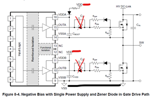
I need some clarification regarding single power supply example in figure 8.4, page 33 of the UCC21550 datasheet.

1) In the  single power supply configuration, VDD (12V Isolated power supply) is supplied both to VDDA and VDDB?

2) VSSA is connected to the  the Switch node (V_DS)?

3) The Negative of the VDD (GND) is connected to VSSB

4) The Negative of the VDD (GND) is the same GND as the Low side MOSFET?

5) The Cz and Vz components are not required in the circuit?

6) The ROFF values needs to be lower than RON resistor?

Kind regards,

Bright

Kind regards,

Bright

  • Hi Bright,

    1. Yes, a single supply is used to power both VDDA and VDDB.
      1. In the figure, a bootstrap is used for VDDA which allows for a single supply to be used.
    2. Correct, VSSA in the figure is connected to the switch node.
    3. Correct, the VSSB is connected to the ground of the secondary side.
    4. Correct, the channel B ground (VSSB) is connected to the LS MOSFET ground on the power stage.
    5. Cz and the Zener diode are not required in this circuit. These are there for setting a negative bias on VSSA.
    6. ROFF typically is set lower than RON to allow a higher sink current when turning off the MOSFET.

    Hope these answer your questions. Feel free to ask any additional questions below.

    Regards,

    Hiroki

  • Hi Hiroki,

    Thank you for your response. 

    Concerning point (5), in the UCC21550 datasheet page 31,

    "When parasitic inductances are introduced by non-ideal PCB layout and long package leads (for example,
    TO-220 and TO-247 type packages), there could be ringing in the gate-source drive voltage of the power
    transistor during high di/dt and dv/dt switching. If the ringing is over the threshold voltage, there is the risk of
    unintended turn-on and even shoot-through. Applying a negative bias on the gate drive is a popular way to keep
    such ringing below the threshold. Below are a few examples of implementing negative gate drive bias."

    This means that the negative gate drive bias is crucial. I am currently having an issue that is been discussed in the thread: 

    UCC21550: Part 2: Half bridge circuit with UCC21550 not working

    Perhaps adding the negative bias at the VSSA/B will help to ensure that no unintended turn on or shoot through due to the high spike seen in the VGS, above the gate threshold. 

    Kind regards,

    Bright

  • Also, on the application example in Figure 8.4, page 33 of the UCC21550

    6)How does the the zener diode Vz and the capacitor Cz generate a negative bias during turn off

    7) What are the values of the zener diode vz and the capacitor Cz?  

    Kind regards,

    Bright

  • Hi Bright,

    I agree that a negative bias voltage would help with adding margin to accidental turn-ons from noise on the output pin. However, I noticed a couple things from the waveforms you provided in the other thread:

    • In no load condition the waveforms are clean.
    • 44V has some noise, but 48V has a lot more.
      • This seems like an issue with the power stage
      • Even if a negative bias is used to add margin to accidental turn-ons, this type of noise would likely introduce other issues. I would like to find the source of this noise.

    Regarding your additional questions:

    6.) After several cycles, the capacitor Cz develops a voltage across it that is clamped by the Zener reverse voltage. The result of this is the output waveforms being shifted down by the voltage charge in Cz. This negative shift adds margin to the threshold voltage to turn on the MOSFET.

    7.) The Zener diode should be selected to have the desired reverse voltage for the negative bias. The capacitor should be selected to be able to hold the charge from the switching cycles. 

    Regards,

    Hiroki

  • Hi Hiroki,

    Thank you for your response

    1) What is the  recommended value for the capacitor Cz?

    ) Is the zener diode in this configuration 5.1V? i.e., in series with the gate drive signal

    Kind regards,

    Bright

  • Hi Bright,

    A 1uF capacitor should be sufficient.

    The Zener diode can be any value that you want to clamp the capacitor to. A 5.1V will work.

    Let me know if you have any additional questions.

    Regards,

    Hiroki

  • Hi Hiroki,

    Thank you. 

    I will update you

    Kind regards,

    Bright