This thread has been locked.

If you have a related question, please click the "Ask a related question" button in the top right corner. The newly created question will be automatically linked to this question.

LP3982: FAULT pin behaviour on start-up

Part Number: LP3982

Tool/software:

Hi, we have just recently switched a LDO part from a MAXIM MAX8860EUA28 to a TI LP3982IMMX-ADJ/NOPB (as per the compatibility claim in your datasheet).
The circuit was misbehaving and after probing around we realised that there is a problem with the /FAULT pin which is not handled correctly on start-up.
It would appear that we cannot use the recommended MAX8860 TI alternative for cascaded power rails.
Our circuit consists of the following:
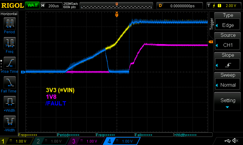
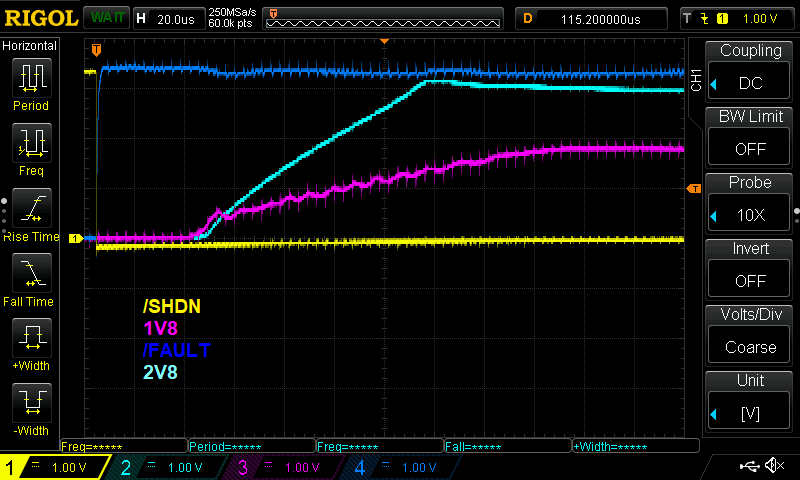
3V3 (always-on) feeds two LDOs, one for a 1.8V rail and another one for a 2.8V rail. 1.8V needs to start before 2.8V, so we cascaded them by having the /FAULT pin of the first LDO (1.8V) connected to the /SHDN pin of the second LDO (2.8V)
The first LDO (1.8V) is controlled with a software driven output connected to the /SHDN pin
The circuit was validated with the Maxim chip and attached are the waveforms of a typical power-up sequence. You can see that the second LDO (2.8V) does not start before the first one (1.8V) enters regulation.

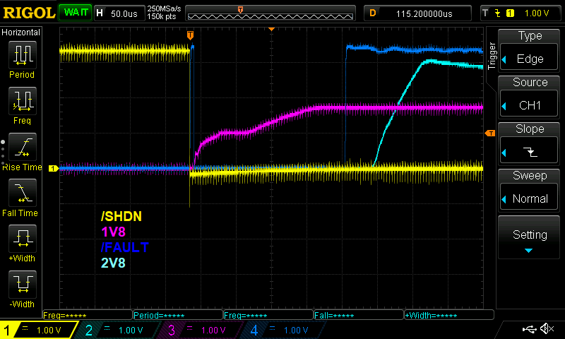
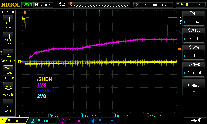
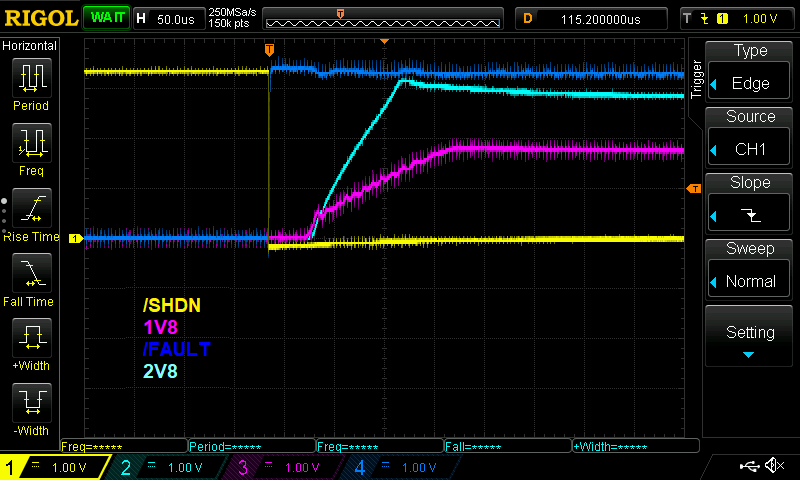
Now with the TI chip in place, we obtain a very different behaviour. Both LDO's power up at the same time. The /FAULT pin does not reflect the state of the 1.8V regulation.


We bought these chips from a reputable distributor and the chip marking is:
28NO
LEVB


Could it a silicon bug with that particular batch? Or a general limitation/incompatibility with the TI chip?

Regards,
Arnauld

  • Hi Arnauld,

    It seems to me to be the way the FAULT behavior was designed and not a bug. The description for the MAX8860 is very similar to the LP3982, but with that said it's not surprising to me that the FAULT pin of the LP3982 does not behave like "power good" by the way it is described. So to answer your question, it looks to be a general incompatibility for this particular use-case. 

    Regards,

    Nick

  • Hi Nick, thanks for your reply.

    It is said in the DS:

    The LP3982 is package, pin, and performance compatible with Maxim's MAX8860, excluding reverse battery protection and dual-mode function.

    It is a pretty poor performance compatibility. It should probably be noted as a warning/limitation in the documentation.

    From the description and looking at the block diagram (7.2), it looks to me that the /FAULT pin is driven low during out of regulation conditions.

    Figure 11 (Power-Up Response) also shows that the /FAULT pin should work in a way I intended to use it. The difference in my application is that VIN is up when the LDO is enabled (/SHDN pin action).

    If it truly turns out an incompatibility with that particular use-case, do you foresee a chip re-spin in the near future?

    Thanks

    Arnauld

  • Hi Arnauld,

    Thanks for pointing out Figure 11; I had overlooked it. I agree that Figure 11 seems to show that the behavior should have satisfied your condition. For the sake of troubleshooting, do you have a way to test whether this would work if VIN is ramped instead of enabling with SHDN? I'm not aware of any EVMs that we have that can fit these old packages on so my testing capability will be more limited than yours. 

    The LP3982 is package, pin, and performance compatible with Maxim's MAX8860, excluding reverse battery protection and dual-mode function.

    It is a pretty poor performance compatibility. It should probably be noted as a warning/limitation in the documentation.

    There seems to be a discrepancy between the reported behavior and what you are seeing because the description of the FAULT behavior and the waveform indicate that this statement is true, but you are seeing different behavior. So, if you can help to identify whether there is truly an issue then I can look into updating the datasheet.

    There is no plan for a re-spin or a 300mm refresh for this device at this moment. It's likely that there won't be one because this isn't a very popular part. 

    Regards,

    Nick

  • Hi Nick,

    Thanks again for your reply.

    As you suggested, I modified my setup to force the /SHDN pin high in order to look at the chip's behaviour when VIN first powers-up.

    Close-up (50us per div)

    This is quite different to figure 11. I note that ramping times in my setup are about 30 times faster (5 ms/div on figure 11, which is pretty slow).

    Both plots (TI's and mine) clearly show that the /FAULT pin is driven low as soon as VIN reaches about 1.5V, however in my case it is released (high) way before VO (1.8V) reaches regulation.

    Regards,

    Arnauld

  • Hi Arnauld,

    I agree that the behavior does not align with the description in the datasheet. It would be nice to see an exact replication of the test - i.e. a slower VIN ramp - to confirm it. Do you have the capability to slow down the VIN ramp any further? 

    Regards,

    Nick

  • Hi Nick,

    I do not have an easy way to slow down VIN ramp.

    Anyway, I believe you guys have all the information needed to replicate the problem at hand, you should at least be able to see what is wrong with the internals of the /FAULT pin at the silicon level.

    Please keep me updated with your findings.

    For now, I am afraid I cannot use the TI alternative part in that specific circuit until a revised version is issued to address the behaviour of the /FAULT pin. Since, according to you, the likelihood of that happening is slim, I would then recommend you add a note in the datasheet to avoid people falling in the same trap.

    Thanks and regards,

    Arnauld

  • Hi Arnauld,

    The difficult issue is that we don't have a board that can fit these legacy packages, so testing them isn't so simple without having some new boards made. I can't make any promises as to how this will be handled but thank you for your time and effort in helping verify the issue.

    Regards,

    Nick