This thread has been locked.

If you have a related question, please click the "Ask a related question" button in the top right corner. The newly created question will be automatically linked to this question.

BQ25798: Ship FET

Part Number: BQ25798
Other Parts Discussed in Thread: BQ25792

Tool/software:

1) Please tell me how to handle the SDRV terminal of the BQ25798 when not using the Ship FET.

    Based on the document below, is it advisable to connect it to GND with a 1000pF capacitor, as with the BQ25792 in the same series?
    Integrated USB Type-C PD and Charging Reference Design for 2-4 Cell Batteries (Rev. B) (ti.com) (https://www.ti.com/lit/ug/tiduey1b/tiduey1b.pdf?ts=1724136248170)

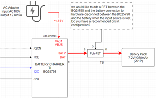
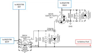
    Also, please let me know if it is okay to handle the BATP and BAT terminals in the same way as the BQ25792 in the diagram below.


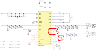
2) I am considering driving the BQ25798's Ship FET using the AUXOFF and _FLT terminal signals of the TPS259470A, which is located after the AC adapter power input.
    The reason for this is that I would like to keep the leakage current from the battery to the BQ25798 to a few tens of μA when the AC adapter is removed and a battery is present while the microcontroller is not operating.
    The image is the configuration in the attached PDF, but is it recommended to use the Ship FET in this way?
    If it is not recommended, please tell me a circuit configuration that can reduce the leakage current to a few tens of μA when a battery is connected.

Regards,
Kagawa

  • Hi Kagawa,

    Regarding 1, no.

    Regarding 2, in battery only mode, the charger pulls current through the BATP pin, i.e. BATP connects to battery side of FET.   The charger Iq isn't different with the required 1000pF cap on SDRV to GND or with SDRV driving the gate of shipFET.   The Iq from the datasheet is shown below:

    If you want to enter ship mode or shutdown mode, you must use a shipFET.  In theory, the shipFET could be controlled by something other than SDRV pin if the host can time the I2C write for ship or shut down mode at the same time as the shipFET is turned off.  It would be easier to use SDRV to control the shipFET.

    Regards,

    Jeff

  • Hi Jeff-san,

    I want to reduce the consumption from the battery to the BQ25798 when the input source is not present.
    We tried to use a Ship FET, but the microcontroller for control is powered from the input source side, so the control to enter Ship Mode is not available in time.
    Therefore, we would like to add a FET between the BQ25798 and the battery connection to hardware disconnect between the BQ25798 and the battery when the input source is lost.
    My idea is shown in the diagram below, do you have a recommended circuit configuration?


    Regards,
    Kagawa

  • Hi Kagawa,

    Although I haven't tested, you could use a PFET with drain at BAT/BATP and an NFET with drain connected to PFET gate.  NFET source at ground and gate at VBUS.

    Regards,

    Jeff

  • Hi Jeff-san,

    We have created a schematic based on your advice and will send it to you in PDF format for your review to ensure that the circuit configuration is correct.
    If you have any concerns, please let us know.

    #14_BQ25798_Charger_schematic_20240822.pdf

    Regards,
    Kagawa

  • Hi Kagawa,

    I do not see any obvious issues on the schematic.

    Regards,

    Jeff

  • Jeff-san,

    By the way, will there be a BMS seminar this year?

    Regards,
    Kagawa

  • Hi Kagawa,

    Not this year.  We are moving to every other year so odd number years.

    Regards,

    Jeff

  • Hi Jeff-san,

    Incidentally, if the configuration is such that the battery and BQ25798 are hardware disconnected when the input source is lost, as in this case, is there any problem if the Ship FET is not implemented?
    If there is no problem even if Ship FET is not implemented, please let me know the recommended processing method since the SDRV pin will be unused.

    Regards,
    Kagawa

  • Hi Kagawa,

    I reviewed the schematic again and noticed that there is no pull up resistor on the PMOS to turn it off.  This pull up resistor from the battery to PMOS source is required.  It will pull some current from the BAT pin when the NMOS is on (VBUS attached).  When the NMOS is off, the only current through it will be PMOS gate leakage current.

    There is no need for the shipFET with the external PMOS. SDRV pin must be tied to ground with 1000pF cap if not used.

    Keep in mind, using external PMOS instead of IC ship mode and external shipFET, all of charger's registers reset to defaults when input power and battery power are removed.

    Regards,

    Jeff

  • Hi Jeff-san,

    I created a circuit diagram based on your advice. I will send it to you in PDF format, so please review it to make sure there are no problems with the circuit configuration.
    In particular, I would like you to check that the position of the pull-up resistor to turn off the PMOS is appropriate.
    If you have any concerns, please let us know.

    #16_BQ25798_Charger_schematic_20240827.pdf

    Regards,
    Kagawa

  • HI Kagawa,

    The pull up resistor placement is correct.

    Regards,

    Jeff

  • Hi Jeff-san,

    If automatic D+D- detection is not used with the BQ25798, is there any problem with leaving both the D+ and D- terminals floating as shown in the circuit diagram below?
    Also, if the STAT terminal output is not used, is there any problem with leaving the terminal floating?


    Regards,
    Kagawa

  • Hi Jeff-san,

    Additional Questions.

    1) I would like to use the BQ25798 as a single input charger. I would like to get advice on which of the following configurations in the datasheet is appropriate.
        9.3.5.2 VBUS Input Only
        9.3.5.3 One ACFET-RBFET
        Please confirm the battery charge specifications as shown below.
       ・Charging Spec


    ・Voltage and Current Settings Value


    2) Regarding the following two configurations described in the BQ25798 datasheet, what are the advantages and disadvantages of each configuration when used as a single-input charger?
        9.3.5.2 VBUS Input Only
        9.3.5.3 One ACFET-RBFET
        Also, what concerns do you see in operating with the 9.3.5.2 VBUS Input Only configuration?

    Regards,
    Kagawa

  • STAT can be floated as they are open drain outputs.

    D+ D- can be floated if not used. 

  • Hi Kagawa,

    One ACFET-RBFET is required for backup mode "9.3.7.2 Backup Power Supply Mode".

    I do not see any obvious issues in your charging spec or voltage and current values.

    Regards,

    Jared Baxter

  • The circuit configuration you previously suggested disconnects the battery from the BAT and BATP of the BQ25798 in the event of input source loss, but if a battery with over-discharge protection is connected, charging may not begin.
    Is it possible to charge a battery with over-discharge protection in the current configuration?
    If not, can you suggest a circuit configuration that can charge a battery whose over-discharge protection is operating and whose output is stopped?
    We will send you the current circuit diagram and waveforms during measurement for your confirmation.

    <circuit diagram>

    <Waveform when an over-discharged battery is connected and 12.8V is applied to VBUS>


    Regards,
    Kagawa

  • Hi Kagawa,

    That's odd.  The IC should be in trickle charge and provide 100mA through the PFET body diode to pack. V(BAT/BATP) should sit at 2.5V after jumping to CELLS x 2.5V for 1.5 seconds. What do the 798 status and fault registers (REG0x1B to 0x27) report?  What is the minimum voltage required for the pack protector to close?  Did the trickle charge timer expire?  If so, set REG0x0E=0 to disable it.  If you short out the PFET, does the same thing occur?

    Regards,

    Jeff

  • Hi Jeff-san,

    At present, the condition sent on 9/5 can no longer be reproduced. Regarding this, once we have reproduced the situation,
    we will measure the content of the question you asked and collect the register values ​​and send them to you for your confirmation.
    The current situation is that a battery in over-discharge protection state is connected and charging has started, with the transition as shown in the waveform below.
    Is this the intended flow of charging start?
    In addition, the over-discharge protection recovery voltage for this battery is specified to be 5.6V or higher, with a maximum of 6.0V.

    <Waveform when an over-discharged battery is connected and 12.8V is applied to VBUS>


    Regards,
    Kagawa

  • Hi Kagawa,

    The plots look reasonable.  I noticed that my explanation above was slightly incorrect:

    If the protector is open (or no battery attached) the charger is in trickle charge and provides 100mA through the PFET body diode to pack with V(BAT/BATP) at ~2.5V Then V(BAT/BATP) jumps to CELLS register x 2.5V for 1.5 seconds. The charger expects the protector to close during this 1.5s.  After that, the charger starts precharge or fast charge.  

    Regards,

    Jeff