This thread has been locked.

If you have a related question, please click the "Ask a related question" button in the top right corner. The newly created question will be automatically linked to this question.

LMG3422R030: Vsd is Quite Smaller than its Value in the Datasheet

Part Number: LMG3422R030

Tool/software:

Hi Team,

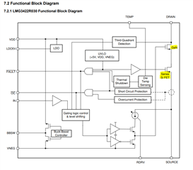
Currently, when customer doing reverse test find that the Vsd is quite smaller than its value in the datasheet, which is shown as below:

Input Current

Ambient Temperature ℃

Voltage V

Current A

Power Loss W

3A

28.201

0.6465

2.9846

1.9295

4A

28.631

0.6639

3.9796

2.6419

6A

28.462

0.7211

5.9688

4.3043

7A

29.344

0.7637

6.9634

5.3176

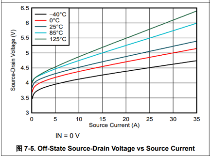
Could you please help check whether there is any problem here? And if, could you please provide your professional advice to customer? Thanks in advance.

BRs,

Francis

  • Hi Francis,

    When they are measuring the Vsd, are they supply VDD voltage to the device?

    Best,

    Kyle Wolf

  • Hi Wolf,

    Not connect, is this the question? If yes, what's the principle? Thanks.

    BRs,

    Francis

  • Hi Francis,

    Kyle is out of office right now so I can help support in the meantime.

    It is very important that the device has power on the VDD pin, otherwise the off-state conditions will not be accurate.

    Please advise your customer to power the VDD supply and retest, let me know if you have any other questions here.

    Thanks,

    Zach

  • Hi Zach,

    I have asked customer to do the evaluation again with the power supply.

    But could you please help provide a internal principle explanation as customer is asking for this.

    Thanks.

    BR,

    Francis

  • Hello,

    Understood, I will clarify for you.

    This device, LMG3422, is a depletion mode GaN FET meaning the device is normally ON and conducting when no VDD is supplied. For safety, we include a silicon FET in series with the GaN so that the device still blocks voltage if no VDD is applied, the diagram is shown below:

    If the customer does not apply VDD to the device, and measures reverse voltage drop, what will happen? The GaN FET portion will be on and conducting, so the only voltage drop there will be from the Rdson of the part (26 mOhm). The silicon FET will conduct through its' body diode and have a voltage drop of roughly 0.7V. This is why the customer sees a voltage drop of about 0.7V at low current and slightly higher voltage drop as the current increases. The increased current causes a higher voltage drop across the depletion mode FET (acting as a resistor with value 26 mOhm).

    If the device is powered on with VDD, the GaN FET will be OFF and reverse conduction will follow as shown in the datasheet.


    Please let me know if you need any further explanation of this point.

    Regards,

    Zach