This thread has been locked.
If you have a related question, please click the "Ask a related question" button in the top right corner. The newly created question will be automatically linked to this question.
Tool/software:
Hi Everyone,
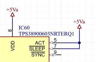
I am using two TPS38900603NRTERQ1 which share an NIRQ Line with a LED and a 560R Resistor pulled to a 3.3V Rail.
There should be a maximum current of 2.7mA flowing. (3.3V - 1.75V LEd)/560R (Assuming all the current flows through one IC only).
This current is allowed according to the absolute maximum ratings, but higher than the Recommended Operating Conditions.
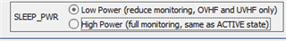
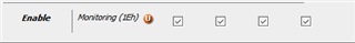
However, all the voltages shown in the Fusion Design Software are 0.2V (x1 Setting) and 0.8V (x4 Setting) and software does not seem to work properly.
Can the slightly higher NIRQ current cause any latch ups?
VDD, ACT and Sleep are connnected to +5V directly.
Thank you.
Kind regards
Moritz
In the first working design the TPS389006004RTERQ1 was used (500uA NIRQ current was lower as well) and in the current design the TPS38900603NRTERQ1. Are there any major differences between those ICs besides threshold voltage and scaling, which lead to the Fusion Design Software no longer working ( 0.2V)?
Hello Mortiz,
There is no issue with the 2.7 mA current, the recommendation operating conditions will be updated to +/- 5mA in the next datasheet revision. I apologize for the fusion digital software, there is currently a bug which does not allow the interface to update the channel count. We are currently working on a fix for this problem. In the meantime is there an I2C instruction i can assist with?
Regards,
Oscar Ambriz
Hello Oscar,
I am glad to hear that, this makes it easier to use an LED to indicate a fault at the NIRQ pin.
Regarding my comment.
Is there any major difference between the two chip versions? I am afraid the ACT/SLEEP - Edge Triggered might cause the issue ?
If I click Sleep_PWR the button is reset immediately.
Thank you very much.
Is there a way to wake the IC up via the Fusion Design Software?
Kind regards
Moritz
Hello Moritz,
I apologize, missed your question in my first response
1. Is there any major difference between the two chip versions? I am afraid the ACT/SLEEP - Edge Triggered might cause the issue ?
You are correct one is level triggered and one is edge triggered. The level trigger device will perform the action so long as the voltage at the pin reaches the required threshold. When edge triggered a well defined edge will need to be provided to the pin for an action to occur.
Secondly, the TPS38900603NRTERQ1 device has PEC enabled, meaning that a PEC byte will need to be provided when performing an I2C write. More information is provided in the PEC section of the datasheet. I have attached a sheet which assist in calculating the PEC byte.
2. If I click Sleep_PWR the button is reset immediately.
What device are you using during in this test? if it is TPS38900603NRTERQ1 a PEC byte will need to be added to the write transaction. Are you performing this operation while polling the device, the software can only write when not polling.
3. With the TPS389006004RTERQ1 this behavior was visible when I disabled the monitoring.
When using the GUI the user needs to click on write to hardware to write to the device. As i mentioned before the GUI has a bug which does not allow the monitor count to update to the proper ch count. TPS389006004RTERQ1 is a 6 ch device not a 4 ch device. I have a attached an instruction sheet to help you perform an I2C transaction without the GUI.
Regards,
Oscar Ambriz
Hi Oscar,
thank you very much.
The straight forward way is even with the SMBus / I2C / SAA Tool not possible:
I am not able to change Registers;
08:56:07.060: SAA #1: I2CWrite (Address 52d, Cmd 0xF0, 0x01): ACK // Change Bank
08:56:11.133: SAA #1: I2CRead (Address 52d, Cmd 0x1E): ACK 0x00 // Read Vmon , all are 0
08:56:21.973: SAA #1: I2CWrite (Address 52d, Cmd 0x1E, 0x01): ACK // Change Vmon , to Ch1 Active
08:56:26.683: SAA #1: I2CRead (Address 52d, Cmd 0x1E): ACK 0x00 // Read all are still 0
I tried to use PEC in the I2C Tool, but I was not able to to send the PEC byte after the message.
However according to the 0x11 Register PEC is disabled.
According to the datasheet PEC should be enabled for the TPS38900603NRTERQ1.
09:42:15.344: SAA #1: I2CWrite (Address 52d, Cmd 0xF0, 0x01): ACK // Change Bank to 1
09:42:16.541: SAA #1: I2CRead (Address 52d, Cmd 0x11): ACK 0x00 // All are 0
I tried to send if afterwards via the Send byte feature, but still no luck.
09:51:45.908: SAA #1: I2CWrite (Address 52d, Cmd 0xF0, 0x01): ACK // Change Bank to 1
09:52:03.830: SAA #1: SendByte (Address 52d, Cmd 0x87): ACK // PEC
09:52:14.843: SAA #1: I2CRead (Address 52d, Cmd 0x22): ACK 0x00 // Read if PEC is disabled
09:52:31.616: SAA #1: I2CRead (Address 52d, Cmd 0x1E): ACK 0x00 // Read Vmon, all are 0
09:52:38.142: SAA #1: I2CWrite (Address 52d, Cmd 0x1E, 0x01): ACK // Write enable Ch1
09:52:51.864: SAA #1: SendByte (Address 52d, Cmd 0x12): ACK // PEC
09:52:58.853: SAA #1: I2CRead (Address 52d, Cmd 0x1E): ACK 0x00 // Read Vmon, all are 0
It seems like the IC is an read-only mode and nothing can be changed via the GUI or the I2C Tool.
Kind regards
Moritz
Hello Moritz,
I apologize for the confusion i should of mentioned the use of the PEC bite, the instructions i provided were tailored to the TPS389006004RTERQ1 variant. Now that i know test are being done using TPS38900603NRTERQ1, can you please perform the following sequence (assuming device address is 0x34, based on your comments above) :
I2C Write: Address: 0xF0 Data: 0x3487 (type in the whole 3487 number, the software will automatically do the multibyte write)
I2C Read: Address: 0x1E, this should now result in the 0x3F data
2C Write: Address: 0xF0 Data: 0x001E (again use the entire number when performing the write command.
This should disable the monitoring now.
Regards,
Oscar Ambriz
Hi Oscar,
don't worry.
However, this approach did not work as well.
The address is still 0x34 and if I send the PEC the messages are NACK.
Regular messages are ACK.
13:13:04.012: SAA #1: I2CWrite (Address 52d, Cmd 0xF0, 0x3487): NACK
13:13:21.732: SAA #1: I2CRead (Address 52d, Cmd 0x1E): ACK 0x00
13:14:05.725: SAA #1: I2CWrite (Address 52d, Cmd 0xF0, 0x001E): NACK
13:14:09.115: SAA #1: I2CRead (Address 52d, Cmd 0x1E): ACK 0x00
Kind regards
Moritz
Hello Moritz,
I mistakenly copied the device address and not the data entry, the correct sequence is below. Just to confirm your device address is 0x34 correct?
I2C Write: Address: 0xF0 Data: 0x0187 (Enter Bank One of register map)
I2C Read: Address: 0x1E (This command will read from address 0x1E of Bank One, should result in 0x3F)
2C Write: Address: 0x1E Data: 0x0015 (This will write a value of 0x00 to register 0x1E of Bank One as intended)
I2C Read: Address: 0x1E (This command will read from address 0x1E of Bank One, should result in 0x00 now that we have performed the write operation)
Regards,
Oscar Ambriz
Hi Oscar,
perfect, I am now able to read the voltage via the polling feature:
08:00:00.859: SAA #1: I2CWrite (Address 52d, Cmd 0xF0, 0x0187): ACK
08:01:16.827: SAA #1: I2CWrite (Address 52d, Cmd 0x1E, 0x0112): ACK
08:01:22.188: SAA #1: I2CRead (Address 52d, Cmd 0x1E): ACK 0x01
08:04:23.704: SAA #1: I2CWrite (Address 52d, Cmd 0x1E, 0x0F38): ACK
08:04:27.193: SAA #1: I2CRead (Address 52d, Cmd 0x1E): ACK 0x0F
08:04:58.481: SAA #1: I2CRead (Address 52d, Cmd 0x1E): ACK 0x0F
Why was it not possible to change settings via the GUI with PEC enabled ?
Thank you very much.
Kind regards
Moritz
Hello Moritz,
I apologize the thread was closed on my end. Unfortunately the GUI does not currently calculate the PEC byte and thus was not satisfying the requirement. We are actively working to update the GUI, with plans to release a major update by the end of the year.
Regards,
Oscar Ambriz
Hi Oscar, thank you for the clarification. This explains a lot
Kind Regards
Moritz