This thread has been locked.

If you have a related question, please click the "Ask a related question" button in the top right corner. The newly created question will be automatically linked to this question.

TPS650864: Regarding PS_POR_PB_B

Part Number: TPS650864

Tool/software:

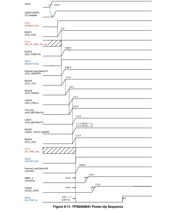
We are using TPS6508641RSKT in our design. We have connected a push button switch to pin CTL1( PMIC implementation is as per document scea113,fig 6.1).We want to know if we can use a AND gate output to the CTL1 pin. input to the AND gates to be PS_POR_PB_B and VCCINT_PG(frpm buck). Would this be ok? Any failure on buck providing 0.72V can result in reset of PMIC. Would this be beneficial for the design? Please let us know. 

  • Hi Prema, 

    For the configuration you are using in fig 6.1 of SCEA113 with TPS6508641RSKT, the main power enable is CTL4, not CTL1.
    So having the AND gate output on CTL1 would not have the effect of resetting the PMIC. 

    (Refer to the power-up sequence Figure 8-11 of the TPS650864x Datasheet)

    CTL1 is controlling the PS_POR_B signal (GPO3 pin output). So with this proposed AND gate, any failure on the buck would result in a reset of the SoC, but not the PMIC itself. 

    There is not a dedicated "reset" function for the TPS650864x. 
    The main power enable for TPS6508641 is CTL4, so if your goal was to power off the PMIC when the buck fails, 
    the AND gate inputs should be POWER_EN and VCCINT_PG and output will be to CTL4.

    The implementation of an AND gate should be ok, but it is not absolutely necessary. 

    Hope this helps to clarify.

    Best Regards,
    Sarah