Tool/software:
Hello.
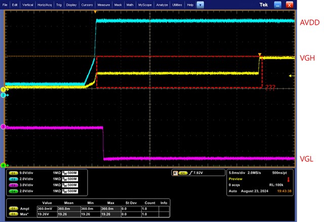
The final output voltage is output at the designed value.(AVDD 9.6V, VGH 18V, VGL -5V)
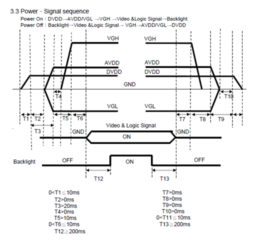
The LCD sequence didn't seem to match, so I checked it with a scope.

It was discovered that the voltage rise of VGH was not normal.
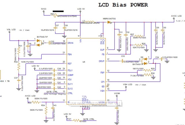
I tried changing the cap of the DLY2 pin, but the start section is not delayed properly.
I want to eliminate the voltage range from 0 to 9V.
The schematic is as follows:

Please check.
Thanks.


