This thread has been locked.

If you have a related question, please click the "Ask a related question" button in the top right corner. The newly created question will be automatically linked to this question.

TPSM365R6: Can VOUT or SW pins be used to synchronize clock signal to LM76002?

Part Number: TPSM365R6LM76002
Other Parts Discussed in Thread: LM76002

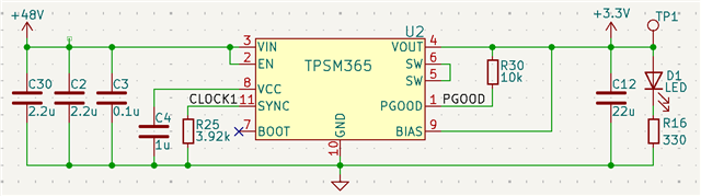
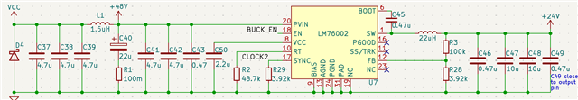
I'm working on a design where a 48V DC source needs to be converted to both 3.3V/0.5A using the TPSM365R6 and 24V/2A using the LM76002. The 3.3V output powers a microcontroller that controls the ENABLE pin of the LM76002, allowing it to save power when the 24V output is not needed. Due to limited board space, I'd like to use a single EMI filter for both buck converters, which I understand would require synchronizing their clock frequencies.

According to the application report "Synchronizing DC/DC Converters in a Power Tree" (Section 1.4 https://www.ti.com/lit/an/slvaeg8/slvaeg8.pdf?ts=1724355001771), it's possible to synchronize the clocks of two buck converters by connecting the switch node voltage of the one converter (in this case, the TPSM365R6 at 3.3V) to the sync pin of the second converter (LM76002). However, the report notes that "Depending on the input and output voltage ratio, the switching waveform can be used directly as a clock reference for the other converter."

Given the significant voltage ratio (48V/3.3V) the expected duty cycle of the TPSM365R6 is 8.25%. I'm unsure if this synchronization strategy will work effectively. Ideally, I'd like to keep the switching frequency around 400-500 kHz for better efficiency.

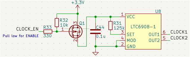
If this approach isn't feasible, I'm open to other suggestions that would allow the use of a single EMI filter. One option might be using an external clock source, powered by the 3.3V output, though this would require additional components. Alternatively, I'm open to considering different buck converters, perhaps those with a clock output pin.

Thank you.

  • Hi Daan,

    The idea proposed will work but as you stated, the duty cycle can be an issue. Also, the SYNC pin has an ABS MAX rating of 5.5V and the part must be in CCM and not in DCM so the SW signal from the first device exhibits a "clock" like signal without any ringing of the node during DCM. I think going with an external clock source will be your best bet. I don't believe we have parts with external clock out unless it is a part that is meant for multi-phasing.

    Ben   

  • Hi Ben, 

    Thanks for your quick and insightful answer. Is it possible for the external clock IC to be powered by one of the bucks that is driven by that IC (a little bit of a chicken egg problem)? Do you have a recommendation for an external clock IC? Preferably with spread spectrum capability

  • Hi Daan,

    I dont think that is possible. As you stated, it is the chicken and egg problem. Regarding the external clock IC, it will be best if you ask the clocking apps team on E2E.

    Ben

  • Thank you Ben. In the datasheet Section 9.3.6.1 (Pulse-Dependent MODE/SYNC Pin Control) there is mention of some behavior change dependent on the received signal on the SYNC/MODE pin, but I'm not sure if I fully understand its behavior. Would it be possible for the TPSM365R6 to initially use the internal clock at startup, and then automatically switch to the external clock source once the external clock IC is powered by the TPSM365R6?

  • Hi Daan,

    Basically, Section 9.3.6.1 describes the various input behavior that TPSM365R6 can tolerate. The cases are:

    1. Changing on the fly from PFM to FPWM and vice versa.
    2. Going from SYNC operation to Auto mode
    3. Going from SNYC operation to FPWM mode.

    To answer your question, I am not sure about your idea but it is definitely a good idea to try it. This is what I would do:

    • The MODE/SYNC pin wound need to have a resistor connected to GND. This would emulate a "low" signal to the MODE/SYNC pin. This would enable the part in AUTO mode.
    • Once the TPSM365R6 is operating, I would use the PGOOD pin to indicate that the output voltage is up at the programmed voltage. I would use the signal of the PGOOD pin to enable the external clock source. The output of the external clock source should be strong enough to drive the MODE/SYNC pin with a pulldown resistor.
    • My concern is how will the system power down safely? Maybe adding a logic gate at the EN input to the external clock source to shut the output off and the MODE/SYNC pin will go low by the pulldown resistor.

    Something to think about but I think it is doable.

    Ben   

  • Great ideas! Could you please explain why you would utilize the PGOOD pin instead of directly powering the external clock by the TPSM365R6 3.3V? The clock can operate with supplies from 2.7V to 5.5V. And could you elaborate on the power down concern? Thank you

  • Hi Daan,

    The PGOOD pin will indicate that the output voltage from the TPSM365R6 is above 90% of the 3.3V. You want to establish the power rail first and then start turning on the external clock. Again, establishing proper sequencing is important. You can definitely try it without the PGOOD pin. No harm is trying both options.

    Ben 

  • Hi Daan,

    If there are no further questions, please click on "resolved" to close the thread. Thanks,

    Ben

  • Hi Ben,

    Even though my original question has been answered, I have a follow-up question for which it doesn't make sense to start a new topic. In the datasheet of the TPSM365R6: Table 9-6. Switching Frequency Versus Output Voltage (IOUT = 600 mA) voltage ranges are given for input voltages and frequencies. Even though this is for the RT version, should this also be followed for external clock frequencies for the SYNC/MODE versions?

  • Hi Daan,

    Yes, the table applies to external clock frequencies as well.

    Ben

  • Great, thank you. In the LM76002 datasheet '8.2.2.14 Synchronization' it is recommended to add a 50 to 100 Ohm termination resistor to the SYNC pin. Is this also the case for the TPSM365R6? If so, I'm not sure if the external clock is strong enough the drive the SYNC signal with this resistance.

  • Hi Daan,

    I would follow the guidelines in the datasheet. If a termination resistor is not mentioned in the TPSM365R6 datasheet, then it is not needed.

    Ben

  • Hi Ben, 

    Following your advice I have ended up with the following circuit

    At start-up, the TPSM365R6 is in auto-mode at 1 MHz due to the pull-down resistor. 

    Once the 3.3V output is stable and PGOOD is high, a microcontroller can enable the external clock (CLOCK_EN) through a P-channel MOSFET. The LTC6908-1 clock IC has two outputs (180° phase shifted outputs to reduce peak current) set at 800 kHz with spread spectrum functionality. When the clock is enabled the TPSM should now switch to SYNC mode.

    The LM76002 can be enabled from the microcontroller (BUCK_EN) with CLOCK2 providing the clock signal.

    It would be great if you could review this. Both VINs of the bucks are filtered by the same LC filter shown in the LM76002 circuit.

    I especially have my doubts about the pull-down resistors value on the sync pins. The LTC6908-1 datasheet mentions "Oscillator Outputs. These pins can drive 5kΩ and/or 10pF loads. Larger loads may cause inaccuracies due to supply bounce at high frequencies". I assume the pull-down resistors need to be below 5kΩ, so I set them equal to the 3.92k feedback resistor to reduce the BOM. But I cannot find any current drive characteristics in the datasheet, nor any information on this on the buck datasheets. I can always experiment and change them with a prototype, but a calculation to get the value approximately correct would be helpful. The parasitic capacitance should be minimal since the traces will be kept as short as possible. Thank you Ben!

  • Hi Daan,

    I especially have my doubts about the pull-down resistors value on the sync pins. The LTC6908-1 datasheet mentions "Oscillator Outputs. These pins can drive 5kΩ and/or 10pF loads. Larger loads may cause inaccuracies due to supply bounce at high frequencies". I assume the pull-down resistors need to be below 5kΩ, so I set them equal to the 3.92k feedback resistor to reduce the BOM.

    The pull-down resistors need to be greater than 5Kohms, not the other way around. The output of the LTC6908-1 can drive no lower than 5kohms or no higher than10pF loads. Remember, it is the drive strength of the LTC6908-1 and the resistor or capacitor is the load that is seen by the LTC device. 

    The input of the SYNC pin for the 76002 and TPSM365 are usually high impedance so adding a known impedance to GND should be high enough to not load down the output of LTC6908-1.

    Regarding your schematic, the output voltage for the 76002 will be higher than 24V (26.67V). Was that your intent? Other than that, the schematics look good to me.

    Ben 

  • Hi Ben,

    That makes more sense, thank you! Yes the voltage is correct. 

    I appreciate your feedback and help with all my questions.

    Daan

  • Hi Daan,

    No problem. Glad to be of help. :-)

    Ben

  • Hi Ben, 

    How accurate is the feedback voltage (Vfb) of the LM76002? The datasheet specifies a typical value of 1.006 V, which we used to determine our feedback resistor values. However, it also lists a minimum value of 0.987 V, leading to a voltage difference of nearly 0.5 V. Should we expect this variation in practical applications? Is there a way to minimize the deviation from the typical value? Thanks

  • HI Daan,

    The FB voltage spec includes temperature (-40C to 125C) and load operation and it is a reference voltage.  Also, the FB voltage is trimmed during test so 1.006V is the target trim during room temp testing.

    Yes, there will be variation from part to part but it should be minimal. I think the confusion is the FB spec is not just the voltage operation at a single condition but over temp and load.

    Ben

  • Hi Daan,

    If there are no further questions, please close this thread. Also, if you have any questions regarding another parts, please open up a separate thread as these threads are searched on a constant basis and we want the thread to be specific to the part in question. Thanks!

    Ben