Tool/software:
Dear sir,
Please help answer the following questions:
1.The sampling input voltage range of CC ADC defined in the specification is -100mv~100mv, which represents the pin voltage range of SRN and SRP, or the voltage difference range between the two pins.
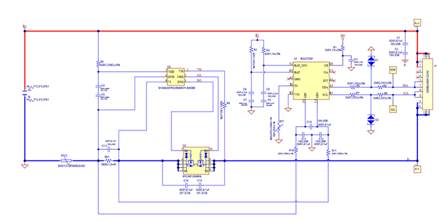
2.In the design of a battery pack protection circuit, when the chip ground is closer to the battery cell, it can more accurately monitor the cell voltage. However, there is a PTC device between VSS and the SRP pins. Please assist in confirming the following operational scenarios:
① Under different current environments, the internal resistance fluctuation of PTC will lead to the change of SRP and SRN voltage to ground. Will it affect the current sampling accuracy of the fuel gauge
② With an external charger voltage of 5V, assuming the internal resistance of the PTC is too high, causing the device to trip, the SRN and SRP voltage may reach -1V. Would this damage the chip?
Note: The schematic is for battery pack protection board, where the PTC is a positive temperature coefficient protection device. Its normal internal resistance is 5mΩ, reaching a maximum of 10mΩ after long-term power cycling, and in the case of abnormal failure, it may reach 50mΩ or greater.